Multi-layer mixed synchronization bonding structure and method for three-dimensional packaging

A multi-layer hybrid and three-dimensional packaging technology, which is applied to semiconductor/solid-state device components, welding equipment, manufacturing tools, etc., can solve problems affecting production efficiency and product reliability, long bonding time, high bonding temperature, etc., to achieve Increase bonding strength and reliability, save time and cost, and improve yield

Active Publication Date: 2011-08-31
NAT CENT FOR ADVANCED PACKAGING
View PDF4 Cites 55 Cited by
  • Summary
  • Abstract
  • Description
  • Claims
  • Application Information

AI Technical Summary

Problems solved by technology

[0006] The present invention aims at the problems of long bonding time and high bonding temperature in existing bonding structures and methods, which seriously affect production efficiency and product reliability, and cause wafer warpage, and provide a multi-layer bonding device for three-dimensional packaging. Hybrid Synchronous Bonding Structure and Method

Method used


Image

  • Multi-layer mixed synchronization bonding structure and method for three-dimensional packaging
  • Multi-layer mixed synchronization bonding structure and method for three-dimensional packaging
  • Multi-layer mixed synchronization bonding structure and method for three-dimensional packaging

Examples


Embodiment Construction

[0032] The principles and features of the present invention are described below in conjunction with the accompanying drawings, and the examples given are only used to explain the present invention, and are not intended to limit the scope of the present invention.

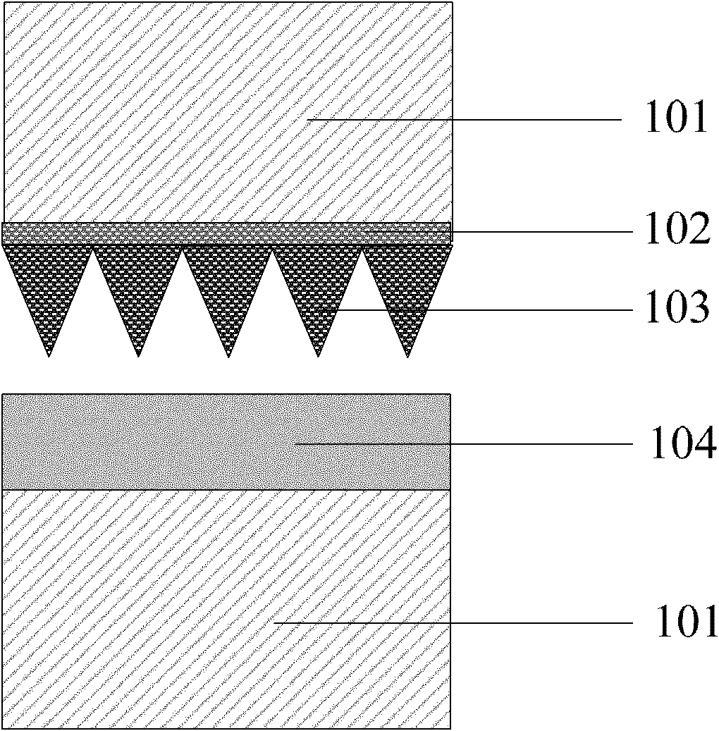
[0033] figure 1It is a structural schematic diagram of the surface of the pad after upper and lower bonding in the embodiment of the present invention. Taking the silicon base plate as an example, metal through holes are formed on the silicon base plate of each layer to form interconnections, and the upper and lower metal interconnection structures are soldered on the surface. A special bonding structure is formed on the disk such as figure 1 As shown, it can be seen from the figure that there is a layer of metal pad 101 on the upper and lower substrates, preferably metal copper, and a hard metal layer 102 can be formed on the upper pad as required, which can be metal chromium, titanium, nickel, etc. The pad is in ...


PUM

PropertyMeasurementUnit
hardnessaaaaaaaaaa
hardnessaaaaaaaaaa

Abstract

The invention relates to a multi-layer mixed synchronization bonding structure and a method for three-dimensional packaging. The method comprises the following steps of: forming a hard metal conical array on a surface of a metallic pad of a substrate to be mixed and bonded; forming a soft metal layer on the surface of the metallic pad of the other substrate to be mixed and bonded; forming dielectric adhesion layers on surfaces of non-metallic pads of the two substrates to be mixed and bonded; aligning the hard metal conical array with the soft metal layer, heating and pressurizing to make thehard metal conical array inserted into the soft metal layer, and combining the dielectric adhesion layers with each other to form a mixed pre-bonding structure; and then heating, forming an intermetallic compound in the hard metal conical array which is inserted into the soft metal layer, and solidifying and combining the dielectric adhesion layers. Compared with the conventional bonding method, the method provided by the invention has the advantages that: yield is high; bonding time is saved; cost is reduced; and the reliability of a product is improved at the same time.

Description

technical field [0001] The invention relates to a multi-layer hybrid synchronous bonding structure and method for three-dimensional packaging, belonging to the technical field of microelectronic packaging. Background technique [0002] With the development of people's requirements for electronic products in the direction of miniaturization, multi-function, and environmental protection, people strive to make electronic systems smaller and smaller, with higher integration, more functions, and stronger . As a result, many new technologies, new materials, and new designs have emerged. For example, technologies such as three-dimensional stacked packaging are typical representatives of these technologies. This structure can directly stack multiple bare chips or substrates by bonding to achieve three-dimensional The metal interconnection structure in the direction greatly reduces the interconnection distance and increases the transmission speed, thereby realizing the integration o...

Claims


Application Information

Patent Timeline
Patent Type & Authority Applications(China)
IPC IPC(8): H01L21/60H01L21/603B23K1/00H01L23/00H01L23/488
CPCH01L2924/09701H01L2224/83855H01L2224/16227H01L2224/16503H01L2224/0557H01L2224/73103H01L2224/9211H01L2924/01327H01L2924/01055H01L2224/16225H01L2224/8181H01L2224/30181H01L2224/73203H01L2224/81395H01L2924/01079H01L2224/13019H01L2224/16146H01L2224/3012H01L2224/17181H01L2224/2919H01L2924/01322H01L2224/131H01L2224/9205H01L2224/81203H01L2224/81193H01L2224/13025B23K2201/40H01L25/50B23K1/0016H01L2224/81986H01L2924/00014H01L2924/0002H01L2224/0401B23K2101/40H01L2924/00012H01L2924/00H01L2224/05552
Inventor 于大全王惠娟
Owner NAT CENT FOR ADVANCED PACKAGING
Why Eureka
Try Eureka