
Semiconductor power device with high-K medium tank

A technology of power devices and semiconductors, which is applied in the direction of semiconductor devices, electrical components, circuits, etc., can solve the problems that the conduction loss of devices is not greatly improved, and the charge imbalance effect in the superjunction drift region is sensitive, so as to increase the process capacity. Poor, avoid charge balance problem, effect of low conduction loss

Inactive Publication Date: 2011-09-14
UNIV OF ELECTRONIC SCI & TECH OF CHINA
View PDF5 Cites 24 Cited by
  • Summary
  • Abstract
  • Description
  • Claims
  • Application Information

AI Technical Summary

Problems solved by technology

The extended trench of this structure is filled with silicon dioxide. Although the dynamic performance of the device is greatly improved, the conduction loss of the device is not greatly improved, and the withstand voltage of this structure has a great influence on the superjunction drift region. The charge imbalance effect is still very sensitive

Method used


Image

  • Semiconductor power device with high-K medium tank
  • Semiconductor power device with high-K medium tank
  • Semiconductor power device with high-K medium tank

Examples


Embodiment Construction

[0036] The present invention will be described in detail below in conjunction with the accompanying drawings.

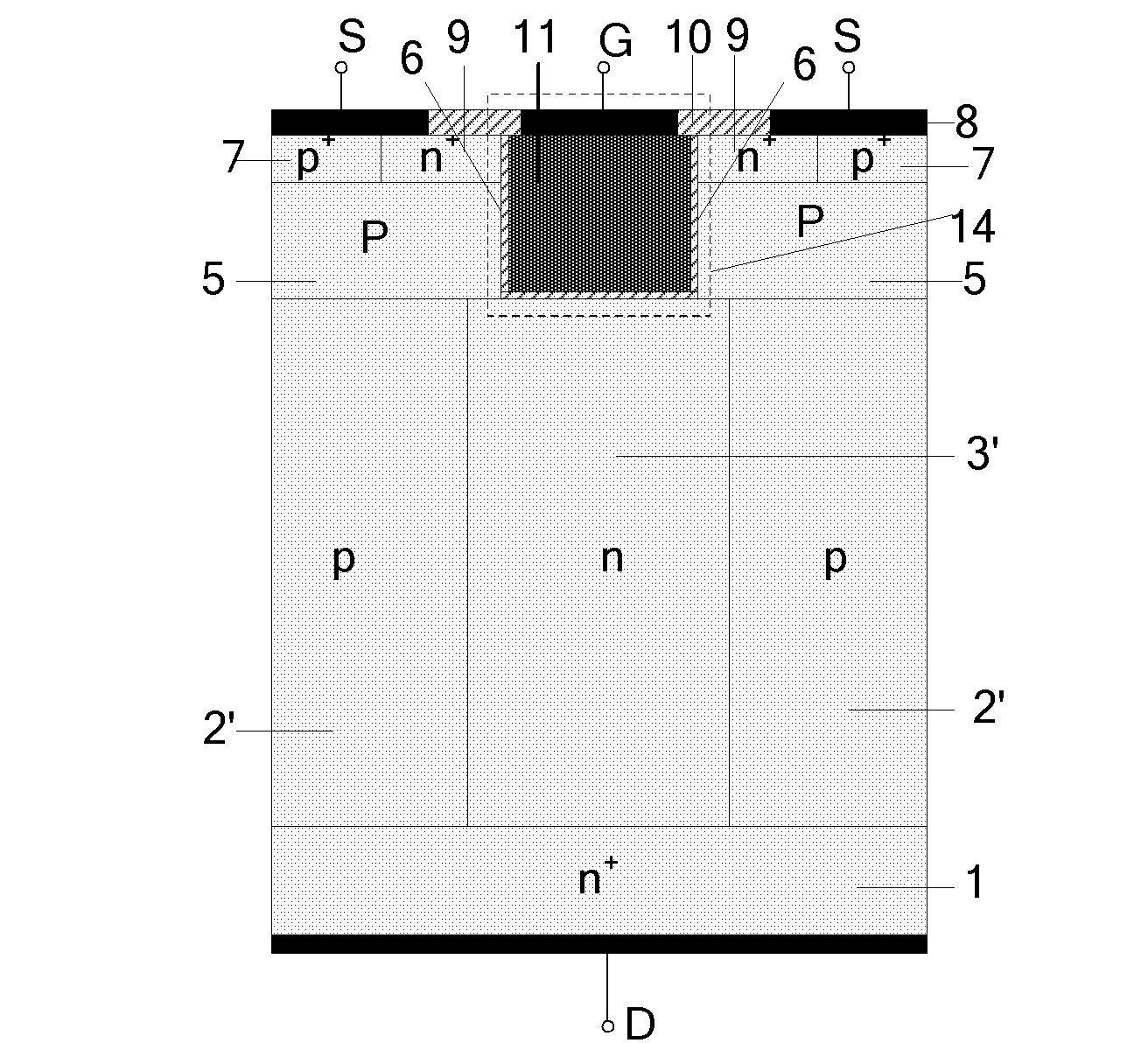
[0037] Conventional super junction trench gate VDMOS structure, such as figure 1 As shown, on the semiconductor substrate 1 is a drift region, the drift region includes alternate p-type semiconductor regions 2' and n-type semiconductor regions 3', the p-type semiconductor regions 2' and n-type semiconductor regions 3' are columnar, also Referred to as a p-column region and an n-column region, the p-type semiconductor region 2' and the n-type semiconductor region 3' form a superjunction. The n-type semiconductor region 3' is located directly below the groove gate structure 14, and the width of the n-type semiconductor region 3' is greater than the width of the groove gate structure. The groove gate structure includes a gate dielectric 6 and a conductive material 11 surrounded by the gate dielectric. The gate electrode G is drawn out. Preferably, the total amount of...


PUM


Abstract

The invention relates to a semiconductor power device with a high-K medium tank, belonging to the technical field of power semiconductor devices. The device comprises a semiconductor substrate, a semiconductor drift region on the semiconductor substrate, and an active area and a trench gate structure on the semiconductor drift region, wherein the semiconductor drift region comprises a first semiconductor area and a second semiconductor area having the same conduction type; the dosage concentration of the second semiconductor area is higher than that of the first semiconductor area, and the width of the second semiconductor area is smaller than that of the first semiconductor area; a high-K medium tank is arranged below the trench gate structure; two ends of the high-K medium tank are contacted with a conductive material of the trench gate structure and the semiconductor substrate respectively, and two sides of the high-K medium tank are contacted with the second semiconductor area; and the drift region consisting of the first semiconductor area and the second semiconductor area are symmetrically distributed at two sides of the high-K medium tank. The semiconductor power device has the advantages of being high in voltage resistance, small in on resistance, low in power consumption, large in process tolerance, simple in manufacturing process and low in cost and the like, and is suitable for being as the power semiconductor device with low power consumption.

Description

technical field [0001] The invention belongs to the technical field of power semiconductor devices, in particular to a low-power semiconductor power device controlled by slot-type MOS. Background technique [0002] Power MOSFET is a multi-subconduction device, which has many advantages such as high input impedance, high frequency, and positive temperature coefficient of on-resistance. These advantages make it widely used in the field of power electronics, greatly improving the efficiency of electronic systems. [0003] The high voltage resistance of the device requires a long drift region and a low doping concentration in the drift region. However, as the length of the drift region increases and the doping concentration decreases, the on-resistance (R on ) increases, the on-state power consumption increases, and the device on-resistance R on There is the following relationship with the breakdown voltage BV: that is, R on ∝BV 2.5 . [0004] With the advancement of the m...

Claims


Application Information

Patent Timeline
IPC IPC(8): H01L29/06H01L29/78
Inventor 罗小蓉姚国亮王元刚雷天飞陈曦葛瑞张波李肇基
Owner UNIV OF ELECTRONIC SCI & TECH OF CHINA
Features
  • Generate Ideas
  • Intellectual Property
  • Life Sciences
  • Materials
  • Tech Scout
  • Unparalleled Data Quality
  • Higher Quality Content
  • 60% Fewer Hallucinations
Learn More