Enhanced AlGaN/GaN HEMT (High Electron Mobility Transistor) device and manufacturing method thereof

An enhancement type, device technology, applied in the fields of semiconductor/solid-state device manufacturing, semiconductor devices, electrical components, etc., can solve the problem of poor performance of GaN integrated circuits, difficult to accurately control the thickness of the AlGaN barrier layer in the gate region, and damage to AlGaN/GaN heterogeneity. junction interface characteristics and other issues, to achieve the effect of simple and controllable process and small gate leakage current

Inactive Publication Date: 2011-09-14
UNIV OF ELECTRONICS SCI & TECH OF CHINA
View PDF7 Cites 14 Cited by
  • Summary
  • Abstract
  • Description
  • Claims
  • Application Information

AI Technical Summary

Problems solved by technology

[0013] Although this method is effective, its biggest problem is that it is difficult to accurately control the thickness of the AlGaN barrier layer in the gate area due to the difficulty in monitoring the etch rate.
[0015] Although this method avoids the disadvantages of the above two methods, its biggest problem is that the F ion implantation of the AlGaN barrier layer in the gate region will destroy the characteristics of the AlGaN / GaN heterojunction interface and degrade the performance of the GaN enhanced HEMT device. As a result, the performance of the developed GaN integrated circuit is poor

Method used


Image

  • Enhanced AlGaN/GaN HEMT (High Electron Mobility Transistor) device and manufacturing method thereof
  • Enhanced AlGaN/GaN HEMT (High Electron Mobility Transistor) device and manufacturing method thereof
  • Enhanced AlGaN/GaN HEMT (High Electron Mobility Transistor) device and manufacturing method thereof

Examples


specific Embodiment approach

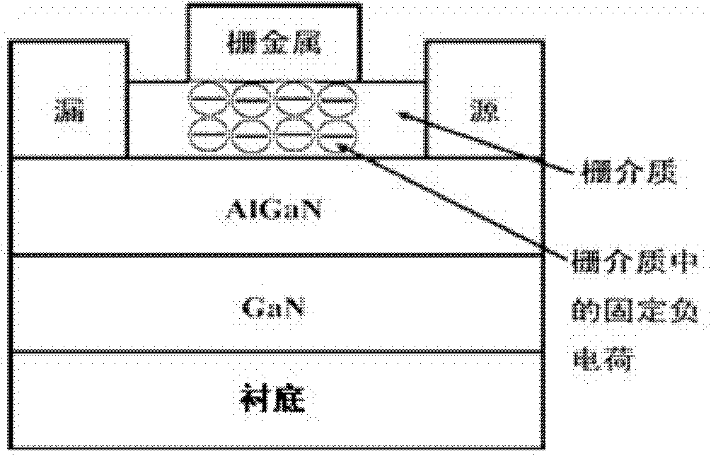
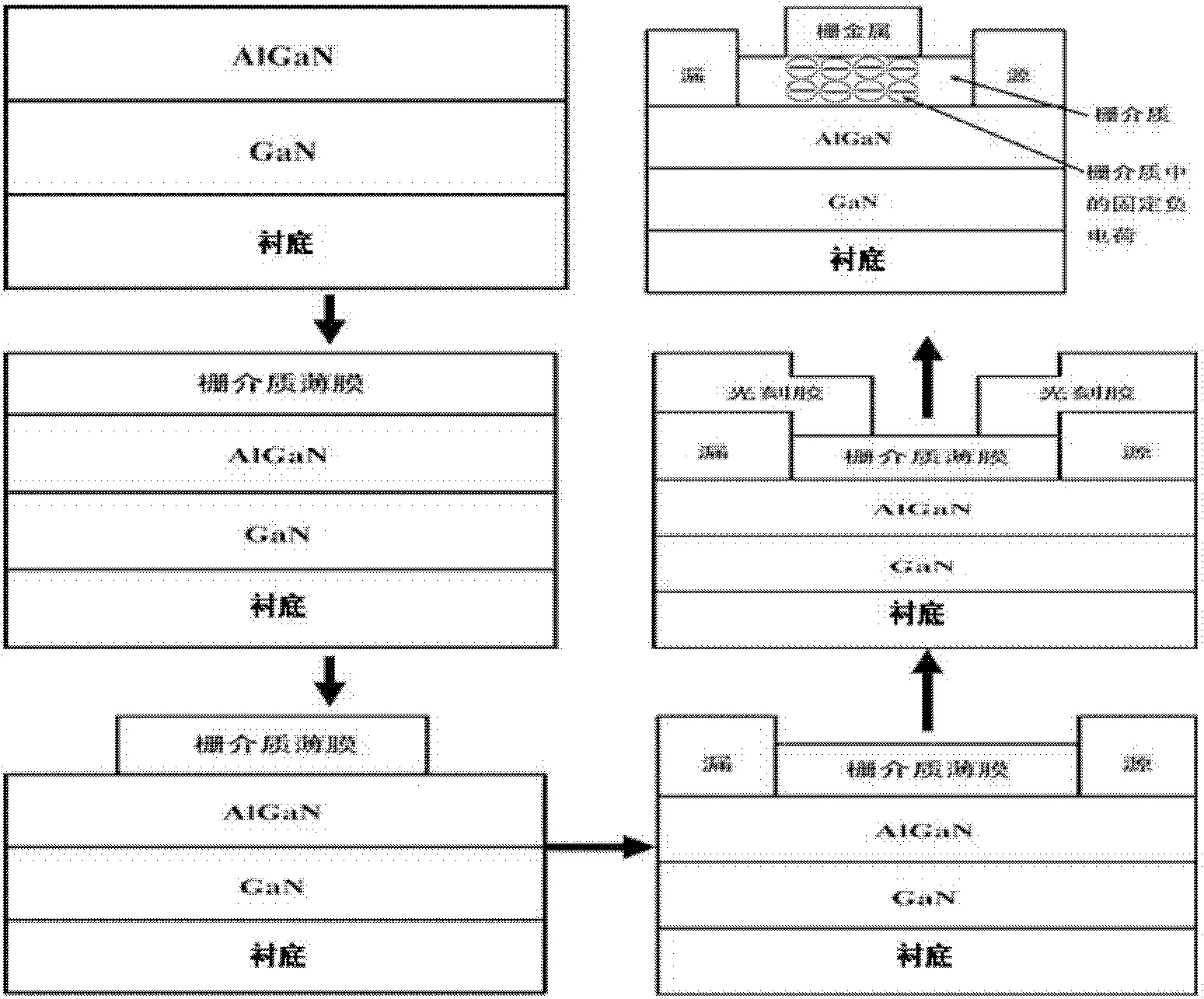
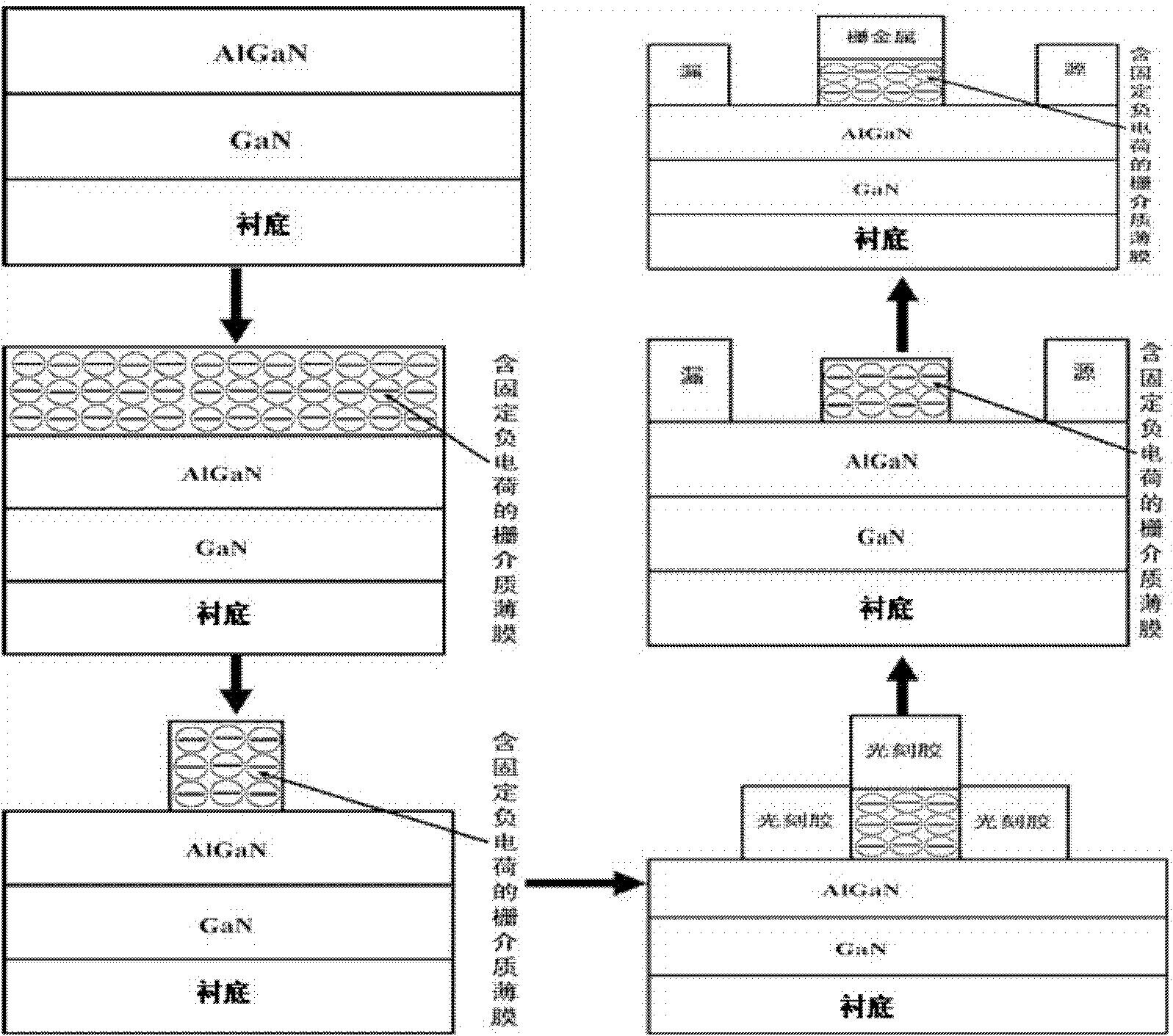
[0045] Using the present invention as figure 2 The process flow shown, using F ion-implanted Al 2 o 3 (hereinafter abbreviated as: F: Al 2 o 3 ) film as the gate dielectric enhancement mode AlGaN / GaN HEMT device, the schematic diagram of the device structure is shown in Figure 6 shown. Its specific implementation is as follows:

[0046] (1), first prepare AlGaN / GaN heterojunction material on sapphire substrate, and then use molecular beam epitaxy (MBE) to deposit a layer of about 10nm thick Al on the surface of AlGaN / GaN heterojunction material 2 o 3 film.

[0047] (2), covered with Al 2 o 3 The surface of the thin-film AlGaN / GaN heterojunction material is spin-coated with photoresist, and the positions of the source region (Source) and the drain region (Drain) are positioned by photolithography, and then the source region and the drain region are positioned with a 1:100 HF solution. Al 2 o 3 The film is etched away. Electron beam evaporation technology is used ...


PUM


Abstract

The invention relates to an enhanced AlGaN/GaN HEMT (High Electron Mobility Transistor) device and a manufacturing method thereof, belonging to the technical field of semiconductor devices. The device comprises an AlGaN/GaN heterojunction structure located on the surface of a substrate and gate, source and drain electrode structures, wherein F ion or Cl ion fixed negative charges are arranged in a gate dielectric film material. In the invention, through introducing the F ion or Cl ion fixed negative charges into a gate dielectric film and controlling the electric charge quantity of the introduced fixed negative charges, the threshold voltage of a transistor is regulated and the enhanced AlGaN/GaN HEMT device with the threshold voltage greater than zero is realized. In the invention, the enhanced AlGaN/GaN HEMT device structure is obtained though a method of introducing the fixed negative charges into the gate dielectric film material; interface characteristics of the AlGaN/GaN heterojunction are not influenced so that the performance degeneration of the device is not caused; the process is simple and controllable and is compatible with the manufacturing process of a depletion mode (normally-on) AlGaN/GaN HEMT device; the source-drain saturation current density and the gate-drain current of the manufactured device for manufacturing a GaN enhanced effect transistor are small; and therefore, the device is particularly suitable for developing a GaN logic circuit.

Description

technical field [0001] The invention belongs to the technical field of semiconductor devices, and relates to a semiconductor field effect transistor and a preparation method thereof, in particular to an AlGaN / GaN heterojunction HEMT device and a preparation method thereof. Background technique [0002] Compared with high electron mobility transistors (HEMTs) based on AlGaAs / GaAs (AlGaAs / GaAs) heterojunctions, HEMT devices based on AlGaN / GaN (AlGaN / GaN) heterojunctions have the following advantages: [0003] 1. The two-dimensional electron gas (2DEG) concentration at the AlGaN / GaN heterojunction interface is relatively high (up to 10 13 em -2 ), which is nearly an order of magnitude higher than the 2DEG concentration at the AlGaAs / GaAs heterojunction interface. Therefore, HEMT devices based on AlGaN / GaN heterojunctions have higher output power densities. As a mass-produced product, the power density of HEMT devices based on AlGaN / GaN heterojunction has reached more than 10W...

Claims


Application Information

Patent Timeline
Patent Type & Authority Applications(China)
IPC IPC(8): H01L29/36H01L29/778H01L21/335
Inventor 刘兴钊陈超李言荣张万里
Owner UNIV OF ELECTRONICS SCI & TECH OF CHINA
Why Eureka
Try Eureka