Polishing composition and polishing method using the same

A technology of polishing composition and compound, which is applied in the field of polishing composition, can solve the problems of high smooth surface for a long time, unable to provide sufficient polishing rate, etc.

Active Publication Date: 2011-09-21
FUJIMI INCORPORATED
View PDF13 Cites 10 Cited by
  • Summary
  • Abstract
  • Description
  • Claims
  • Application Information

AI Technical Summary

Problems solved by technology

However, the problem associated with these methods is that it takes a lot of time to produce a highly smooth surface because these methods do not provide a sufficient polishing rate (removal rate)

Method used


Image

  • Polishing composition and polishing method using the same
  • Polishing composition and polishing method using the same
  • Polishing composition and polishing method using the same

Examples


example 1 and 2 and comparative example 1

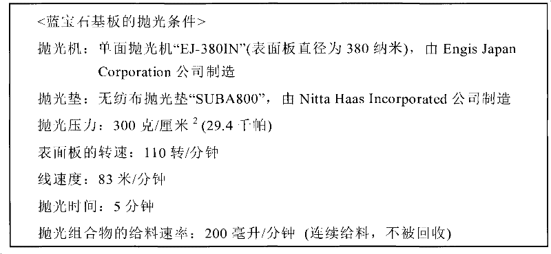
[0032]The polishing compositions of Examples 1 and 2 and Comparative Example 1 were prepared by diluting a colloidal silica sol containing colloidal silica having an average primary particle diameter of 80 nm with water, and adding a pH adjuster as necessary. Each of the polishing compositions of Examples 1 and 2 and Comparative Example 1 contained 20% by mass of colloidal silica. Hydrochloric acid or potassium hydroxide is suitably used as a pH adjuster. Using each of the polishing compositions of Examples 1 and 2 and Comparative Example 1, the surface (c-plane ()) of the sapphire substrate was polished under the conditions shown in Table 1. All sapphire substrates used were of the same type, with a diameter of 52 millimeters (about 2 inches).

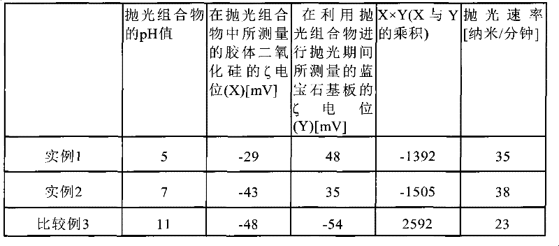
[0033] Table 2 shows the pH value of the polishing composition, the zeta potential value of colloidal silica measured in the polishing composition, and the zeta potential value of the sapphire substrate measured during polishing with...

example 3 and comparative example 2

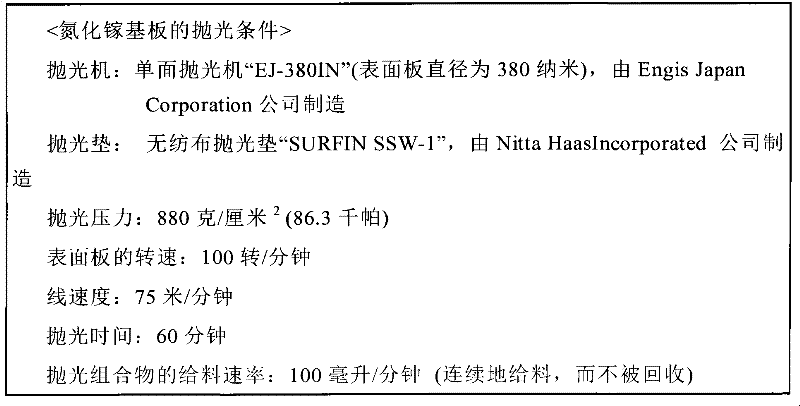
[0040] The polishing compositions of Example 3 and Comparative Example 2 were prepared by diluting the colloidal silica sol containing colloidal silica having an average primary particle size of 80 nm with water, and adding a pH adjuster as needed. Each of the polishing compositions of Example 3 and Comparative Example 2 contained 20% by mass of colloidal silica. Hydrochloric acid or potassium hydroxide is suitably used as a pH adjuster. Using the polishing compositions of Example 3 and Comparative Example 2, the surface (Ga surface) of the gallium nitride substrate was polished under the conditions shown in Table 3. All GaN substrates used are of the same type and have an area of ​​10 mm.

[0041] The pH values ​​of the polishing compositions, the sign of the colloidal silica zeta potential measured in each polishing composition, and the sign of the gallium nitride substrate zeta potential measured during polishing with each polishing composition are shown in Table 4. Befor...

example 4 and 5 and comparative example 3 and 4

[0048] The polishing compositions of Examples 4 and 5 and Comparative Examples 3 and 4 were prepared by diluting a colloidal silica sol containing colloidal silica having an average primary particle diameter of 35 nm with water, and adding a pH adjuster as necessary. Each of the polishing compositions of Examples 4 and 5 and Comparative Examples 3 and 4 contained 5% by mass of colloidal silica. Acetic acid or potassium hydroxide is suitably used as a pH adjuster. Using each of the polishing compositions of Examples 4 and 5 and Comparative Examples 3 and 4, the surface ((100) plane) of the indium arsenide substrate was polished under the conditions shown in Table 5. All of the indium arsenide substrates used were of the same type, with a diameter of 52 mm (approximately 2 inches).

[0049] The pH values ​​of the polishing compositions, the sign of the colloidal silica zeta potential measured in each polishing composition, and the sign of the indium arsenide substrate zeta pote...


PUM

PropertyMeasurementUnit
diameteraaaaaaaaaa

Abstract

A polishing composition contains at least abrasive grains and water and is used in polishing an object to be polished formed of a substrate material for optical devices, a substrate material for power devices, or a compound semiconductor material. The abrasive grains have a zeta potential satisfying the relationship XY!<=0, where X [mV] represents the zeta potential of the abrasive grains measured in the polishing composition and Y [mV] represents the zeta potential of the object to be polished measured during polishing using the polishing composition. The abrasive grains are preferably of aluminum oxide, silicon oxide, zirconium oxide, diamond, or silicon carbide. The object to be polished is preferably of sapphire, gallium nitride, silicon carbide, gallium arsenide, indium arsenide, or indium phosphide.

Description

technical field [0001] The present invention relates to a polishing composition for polishing an object to be polished composed of a substrate material of an optical device, a substrate material of a power device, or a compound semiconductor material. Background technique [0002] The substrate material of an optical device and the substrate material of a power device refer to, for example, ceramics having oxides such as sapphire, nitrides such as gallium nitride, and carbides such as silicon carbide. The compound semiconductor material refers to gallium arsenide, indium arsenide, or indium phosphide, for example. [0003] Because substrates or thin films made of these materials are generally stable against chemical effects such as oxidation, complexation, and etching, processing substrates or thin films by polishing is not easy. Therefore, this processing is usually done by grinding or cutting with hard materials. However, highly smooth surfaces cannot be produced by grin...

Claims


Application Information

Patent Timeline
Patent Type & Authority Applications(China)
IPC IPC(8): C09G1/02C09K3/14H01L21/304H01L21/00B24B29/00B24B37/00
CPCH01L21/02024C09G1/02C09K3/1463B24B37/00C09G1/04C09K3/14H01L21/304
Inventor 森永均玉井一诚浅野宏
Owner FUJIMI INCORPORATED
Why Eureka
Try Eureka