Method for manufacturing glass substrate all buried strip-type optical waveguide stack
A manufacturing method and optical waveguide technology, applied in the direction of optical waveguide light guide, light guide, optics, etc., can solve the problem of not making a fully buried strip optical waveguide stack, increasing optical transmission loss, fiber coupling loss, and increasing the size of the core of the optical waveguide 5 and other issues, to achieve the effect of being suitable for large-scale production, low cost, and low loss
- Summary
- Abstract
- Description
- Claims
- Application Information
AI Technical Summary
Problems solved by technology
Method used
Image

Examples
Embodiment 1
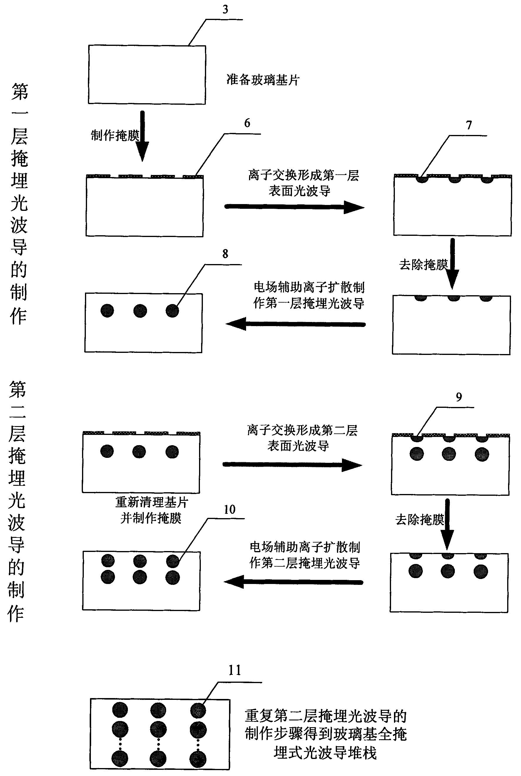
[0033] combine figure 2 As shown, in order to make a double-layer fully buried strip optical waveguide stack, the process steps are as follows:
[0034] 1) preparing a phosphate glass substrate 3;
[0035] Wash the glass substrate 3 with concentrated sulfuric acid, rinse it with deionized water, and dry it in a dust-free environment;
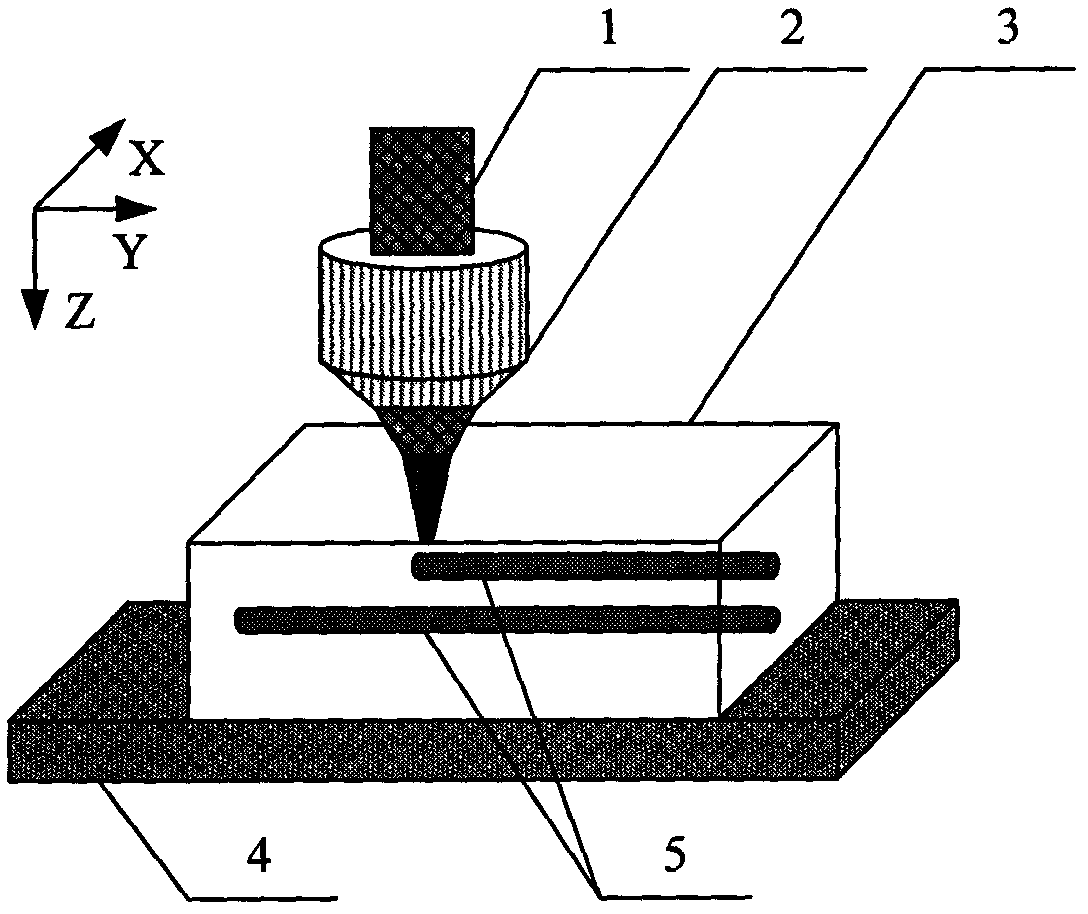
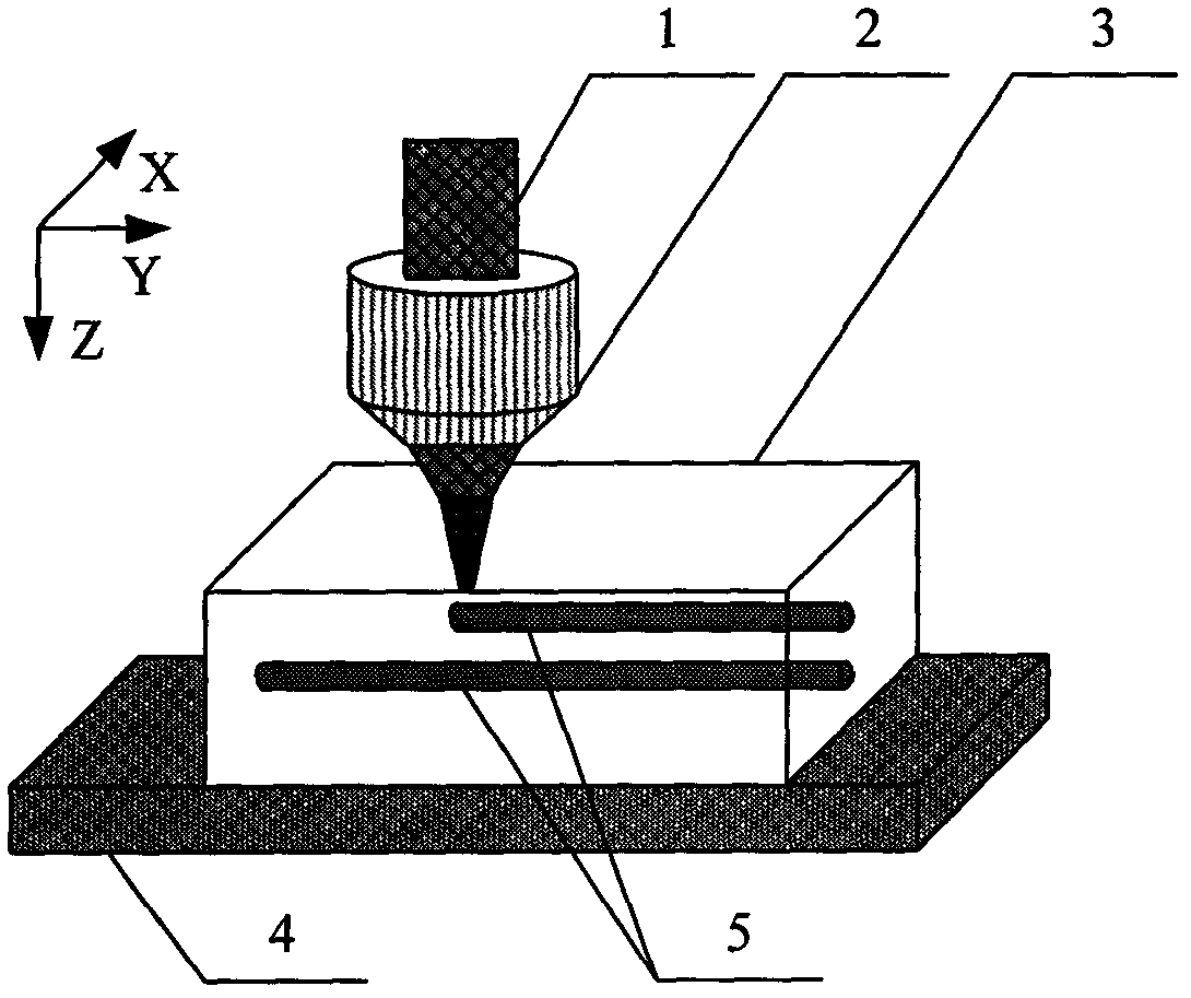
[0036] 2) Fabricate a layer of aluminum film with a thickness of 100nm on the surface of the clean glass substrate 3 by a sputtering process, and fabricate an optical waveguide mask 6 on the surface of the glass substrate 3 through microfabrication techniques such as conventional photolithography and corrosion;
[0037] 3) ion exchange to form the first layer of surface optical waveguide 7;
[0038] Sodium nitrate and silver nitrate in a molar ratio of 100:1 are used as the ion exchange source and heated to make it melt, then the glass substrate 3 is immersed in the exchange source, the exchange temperature is 300°C, and the exchange time is ...
Embodiment 2
[0048] combine figure 2 As shown, in order to make a double-layer fully buried strip optical waveguide stack, the process steps are as follows:
[0049] 1) preparing a silicate glass substrate 3;
[0050] Wash the glass substrate 3 with concentrated sulfuric acid, rinse it with deionized water, and dry it in a dust-free environment;
[0051]2) An aluminum film with a thickness of 100nm is fabricated on the surface of the clean glass substrate 3 through a thermal evaporation process, and an optical waveguide mask 6 is fabricated on the surface of the glass substrate 3 through microfabrication processes such as conventional photolithography and corrosion;
[0052] 3) ion exchange to form the first layer of surface optical waveguide 7;
[0053] Potassium nitrate is used as the ion exchange source and heated to make it melt, the glass substrate 3 is immersed in the exchange source, the exchange temperature is 400 ° C, the exchange time is 5 hours, and finally the glass substrat...
Embodiment 3
[0063] to combine figure 2 As shown, in order to make a double-layer fully buried strip optical waveguide stack, the process steps are as follows:
[0064] 1) preparing a silicate glass substrate 3;
[0065] Wash the glass substrate 3 with concentrated sulfuric acid, rinse it with deionized water, and dry it in a dust-free environment;
[0066] 2) An aluminum film with a thickness of 100nm is fabricated on the surface of the clean glass substrate 3 through a thermal evaporation process, and an optical waveguide mask 6 is fabricated on the surface of the glass substrate 3 through microfabrication processes such as conventional photolithography and corrosion;
[0067] 3) ion exchange to form the first layer of surface optical waveguide 7;
[0068] Sodium sulfate and copper sulfate are used as the ion exchange source in a molar ratio of 1:1 and heated to melt, then immerse the glass substrate 3 in the exchange source, the exchange temperature is 560°C, and the exchange time is...
PUM
 Abstract
Description
Claims
Application Information
 - R&D
- Intellectual Property
- Life Sciences
- Materials
- Tech Scout
- Unparalleled Data Quality
- Higher Quality Content
- 60% Fewer Hallucinations
Browse by: Latest US Patents, China's latest patents, Technical Efficacy Thesaurus, Application Domain, Technology Topic, Popular Technical Reports.
© 2025 PatSnap. All rights reserved.Legal|Privacy policy|Modern Slavery Act Transparency Statement|Sitemap|About US| Contact US: help@patsnap.com