Supercharge Your Innovation With Domain-Expert AI Agents!

Manufacturing method for magnetic tunnel junction structure

A fabrication method and magnetic tunnel junction technology are applied in the field of fabrication of magnetic tunnel junction structures and can solve problems such as increased fabrication cost and the like

Active Publication Date: 2013-05-29
SEMICON MFG INT (SHANGHAI) CORP
View PDF3 Cites 0 Cited by
  • Summary
  • Abstract
  • Description
  • Claims
  • Application Information

AI Technical Summary

Problems solved by technology

[0007] In view of this, the technical problem solved by the present invention is to provide a method for manufacturing a hollow cylindrical MTJ unit, so as to reduce the defects in the prior art that the manufacturing cost increases because the inner diameter of the hollow cylindrical MTJ unit is too small

Method used


Image

  • Manufacturing method for magnetic tunnel junction structure
  • Manufacturing method for magnetic tunnel junction structure
  • Manufacturing method for magnetic tunnel junction structure

Examples


Embodiment Construction

[0023] In order to make the object, technical solution and advantages of the present invention clearer, the present invention will be further described in detail below with reference to the accompanying drawings and examples.

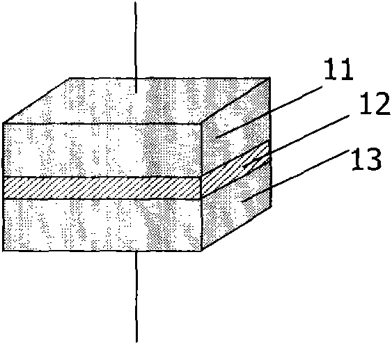
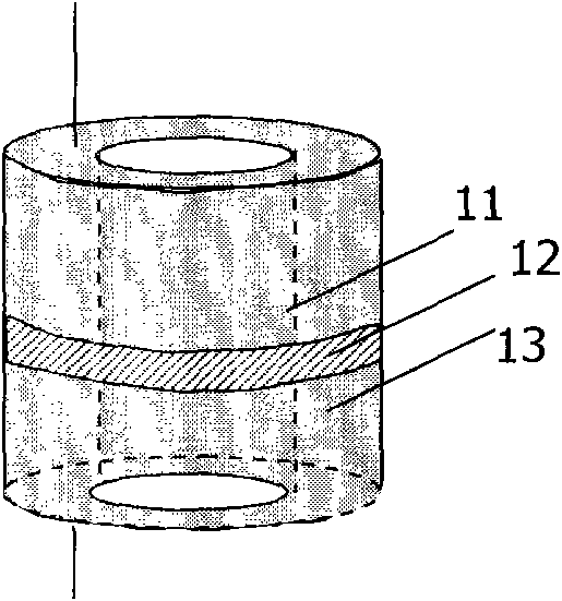
[0024] The present invention forms a metal layer on the side wall of the patterned second mask layer, diffuses metal ions in the metal layer along the second mask layer through an annealing process, increases the width of the metal layer, and etches and removes the gap between the metal layers. The second mask layer of the metal layer exposes the cylindrical part between the metal layers, and then, using the metal layer as a mask, removes the first mask layer and part of the MTJ composite structure between the metal layers to form a hollow The cylindrical MTJ unit.

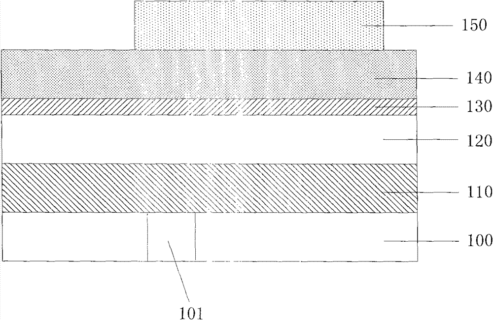
[0025] Reference attached image 3 As shown, a semiconductor substrate and a dielectric layer 100 on the semiconductor substrate are provided. Transistors and interconnection structures fo...


PUM

PropertyMeasurementUnit
widthaaaaaaaaaa
widthaaaaaaaaaa
thicknessaaaaaaaaaa

Abstract

The invention discloses a manufacturing method for an MTJ (Magnetic Tunnel Junction) unit. The method comprises the steps of providing a semiconductor substrate and a dielectric layer on the semiconductor substrate; forming on the dielectric layer an MTJ structure comprising in order a fix magnetosphere, a tunnel barrier layer and a free rotation magnetosphere; forming in order a first mask layerand a second mask layer on the MTJ structure; patterning the second mask layer; forming a metal layer on the sidewall of the second mask layer, annealing to make the metal layer diffuse along the second mask layer; etching to remove the second mask layer on the metal layer; using the metal layer as a mask, etching the first mask layer and the MTJ structure to the semiconductor substrate and removing the metal layer. According to the method, a small-size circle annular MTJ unit can be manufactured with routine lithography equipment.

Description

technical field [0001] The invention relates to a manufacturing technology of a semiconductor device, in particular to a manufacturing method of a magnetic tunnel junction (MTJ) structure. Background technique [0002] MRAM (Magnetic Random Access Memory) is a non-volatile magnetic random access memory. It has the high-speed read and write capabilities of static random access memory (SRAM), high integration of dynamic random access memory (DRAM) and power consumption far lower than DRAM, compared with flash memory (Flash), with the use of time Increase performance without degradation. Due to the above-mentioned characteristics of MRAM, it is called universal memory and is considered to be able to replace SRAM, DRAM, EEPROM and Flash. [0003] Unlike traditional random access memory chip fabrication technology, data in MRAM is not stored in the form of charge or current, but in a magnetic state, and is sensed by measuring resistance without disturbing the magnetic state. M...

Claims


Application Information

Patent Timeline
Patent Type & Authority Patents(China)
IPC IPC(8): H01L43/12H10N50/01
Inventor 邹立罗飞
Owner SEMICON MFG INT (SHANGHAI) CORP
Features
  • R&D
  • Intellectual Property
  • Life Sciences
  • Materials
  • Tech Scout
  • Unparalleled Data Quality
  • Higher Quality Content
  • 60% Fewer Hallucinations
Learn More