
Adhesive tape for wafer processing

A wafer processing and adhesive tape technology, which is applied in the direction of adhesives, film/sheet adhesives, electrical components, etc., can solve the environmental load and other problems, and achieve the effect of low environmental load and sufficient shrinkage

Active Publication Date: 2014-09-03
FURUKAWA ELECTRIC CO LTD
View PDF13 Cites 0 Cited by
  • Summary
  • Abstract
  • Description
  • Claims
  • Application Information

AI Technical Summary

Problems solved by technology

However, when the above-mentioned polyvinyl chloride tape is incinerated after use, chlorinated aromatic hydrocarbons such as dioxin and its analogues may be generated, which may impose a load on the environment.

Method used


Image

  • Adhesive tape for wafer processing
  • Adhesive tape for wafer processing
  • Adhesive tape for wafer processing

Examples


Embodiment 1

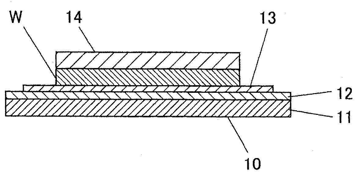
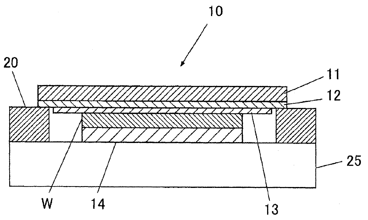
[0192] (Preparation of Base Film 11)

[0193] Zinc ionomer a (density 0.96g / cm3) of ethylene-methacrylic acid-ethyl methacrylate (mass ratio 8:1:1) terpolymer synthesized by free radical polymerization 3 , zinc ion content of 4% by mass, chlorine content of less than 1% by mass, Vickers softening point of 56°C, and melting point of 86°C) were melted at 140°C and molded into a long film with a thickness of 100 μm using an extruder. This produces the supporting substrate 1 for forming the substrate film 11 .

[0194] (Preparation of Adhesive Composition 1)

[0195]An acrylic copolymer (molecular weight: 600,000, hydroxyl value: 4.7 mgKOH / g, acid value: 0.2 mgKOH / g) was obtained by radically polymerizing butyl acrylate, 2-hydroxyethyl acrylate, and acrylic acid. With respect to 100 parts by mass of the acrylic copolymer, 30 parts by mass of trimethylolpropane triacrylate was added as a photopolymerizable cured product, 2 parts by mass of CORONET L (manufactured by Japan Polyure...

Embodiment 2

[0202] (Preparation of Base Film 11)

[0203] Zinc ionomer b (density 0.95g / cm2) of ethylene-methacrylic acid (mass ratio 9.5:0.5) binary copolymer synthesized by free radical polymerization 3 , a zinc ion content of 2% by mass, a chlorine content of less than 1% by mass, a Vickers softening point of 81°C, and a melting point of 100°C) were melted at 140°C and molded into a long film with a thickness of 100 μm using an extruder. This produces the supporting substrate 2 for forming the substrate film 11 .

[0204] Using the support substrate 2 for forming the substrate film 11, the adhesive composition 1, and the adhesive composition 1, the tape 10 for wafer processing was produced by the same method as in Example 1, which was referred to as Example 2. sample.

Embodiment 3

[0206] (Preparation of Base Film 11)

[0207] Ultra-low density polyethylene ULDPEa (density 0.90g / cm2) synthesized by metallocene polymerization 3 , chlorine content less than 1% by mass, Vickers softening point of 72°C, and melting point of 90°C) are melted at 140°C, molded into a long film with a thickness of 100 μm by an extruder, and then used in a medium-energy electron beam accelerator (中ェネルギ-electron beam accelerator) Electron beams were irradiated with an accelerating voltage of 1 MeV and an irradiation dose of 20 Mrad to fabricate the supporting base 3 for forming the base film 11 .

[0208] Using the support substrate 3 for forming the substrate film 11, the adhesive composition 1, and the adhesive composition 1, the tape 10 for wafer processing was produced by the same method as in Example 1, which was referred to as Example 3. sample.


PUM

PropertyMeasurementUnit
thicknessaaaaaaaaaa
melting pointaaaaaaaaaa
acid valueaaaaaaaaaa

Abstract

The invention provides adhesive tape for wafer processing, which has uniform expansion suitable for application for truncating cement layers through expansion and sufficient shrinkage shown in a heating contraction process and results in no unfavorable conditions due to relaxation after the heating contraction process. The expansive adhesive tape 10 which is suitably applied for truncating a cement layer (13) along the wafer through expansion has a base material film 11 which is made of thermoplastic crosslinking resin provided with a Vickers softening point more than 50 DEG but less than 90 DEG as specified in JIS K7206 and having a stress increased over 9 MPa due to heating contraction.

Description

technical field [0001] The present invention relates to an expandable tape for wafer processing which is used when an adhesive layer is cut along a chip by expansion. Background technique [0002] In the manufacturing process of semiconductor devices such as ICs, the following processes are carried out: the back grinding process of grinding the back of the wafer to make the wafer thinner after the circuit pattern is formed; After using the tape, the dicing process of cutting the wafer into chip units; the process of expanding the tape for wafer processing; the process of picking up the cut chip; and sticking the picked chip on a lead frame or package substrate, etc. or in a stacked package Die bonding (mount) process for laminating and bonding semiconductor chips. [0003] In the above-mentioned back grinding process, a surface protection tape is used to protect the circuit pattern formation surface (wafer surface) of the wafer from contamination. After the backside grindi...

Claims


Application Information

Patent Timeline
Patent Type & Authority Patents(China)
IPC IPC(8): C09J7/02H01L21/683H01L21/78
CPCH01L21/6836
Inventor 三原尚明盛岛泰正
Owner FURUKAWA ELECTRIC CO LTD
Learn More