
Electrooptical probe based on fluid electrooptical materials, and method of using electrooptical probe to detect electric field

An electro-optical material and fluid technology, which is used in electrostatic field measurement, components of electrical measuring instruments, and electrical measurement, etc., can solve the problems of narrow surface field of view of integrated circuits, increased cost of electro-optical systems, and low voltage sensitivity of electro-optical detection systems.

Active Publication Date: 2011-10-05
中科精仪科技(广东)有限公司
View PDF5 Cites 4 Cited by
  • Summary
  • Abstract
  • Description
  • Claims
  • Application Information

AI Technical Summary

Problems solved by technology

In actual use, due to the use of solid-state media, there are several disadvantages as follows: (1) The fringe field of the transmission line or node on the surface of the integrated circuit is usually limited within a few microns from the surface of the circuit, which restricts the positioning of the electro-optical probe. The device puts forward at least sub-micron accuracy requirements, which greatly increases the cost of the electro-optical system
(2) Due to the limited precision of the probe positioning device and the fluctuation of the surface topography of the integrated circuit itself, there is an inevitable air gap between the electro-optic material and the measurement point
Most of the fringe field at the measurement point is shielded in the air gap, resulting in a decrease in the conversion efficiency of electricity to light
(3) The size of the air gap between the electro-optic material and the measurement point cannot be effectively detected, so that the electro-optic conversion efficiency of different measurement points cannot be determined, so that the actual electrical signal of the measurement point cannot be accurately inferred from the measured signal.
(4) The electro-optic coefficient of the solid electro-optic material itself is small (usually the refractive index variation coefficient of the solid electro-optic material is several pm / V), which leads to the low voltage sensitivity of the electro-optic detection system, and a set of low-noise and high-magnification electric weak Signal Measurement System
(5) Due to the low hardness and wear resistance of solid electro-optic materials, multiple measurements or large-area measurements will cause irreversible damage to electro-optic materials
(6) The field of view for observing the surface of the integrated circuit is very narrow
Because the base of the solid probe is usually a cone or an optical fiber, and the tip of the cone or the end face of the optical fiber is only a few tens of microns square, so the observation area of ​​the integrated circuit is only a few tens of microns square during detection. Detection points on the surface cause great inconvenience

Method used


Image

  • Electrooptical probe based on fluid electrooptical materials, and method of using electrooptical probe to detect electric field
  • Electrooptical probe based on fluid electrooptical materials, and method of using electrooptical probe to detect electric field
  • Electrooptical probe based on fluid electrooptical materials, and method of using electrooptical probe to detect electric field

Examples


Embodiment 1

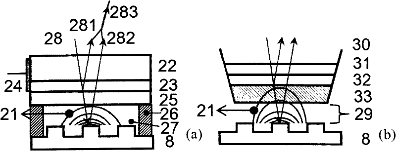
[0066] The structure of the fluid electro-optic probe 7 is as figure 2 As shown in (a), the production steps are as follows:

[0067] 1. Select k9 glass with a thickness of 1mm and optical polishing on the upper and lower surfaces as the material of the transparent substrate 22, and the refractive index for the probe light 1.31 μm is 1.50; use a dicing machine to cut out a square with a size of 2mm*2mm as the fluid electro-optical probe 7 transparent substrate 22;

[0068] 2. On the surface of the transparent substrate 22, use a magnetron sputtering method to sputter an ITO film with a thickness of about 100 nm as the transparent conductive layer 23;

[0069] 3. Wrap the transparent base 22 and the transparent conductive layer 23 layers with tin foil, and expose one side of the side wall of the transparent base 22, evaporate a layer of gold film with a thickness of 0.2 μm on the side wall by thermal evaporation, as the side wall Conductive layer 24, spot welder uses aluminum...

Embodiment 2

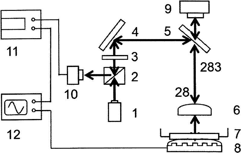
[0074] electro-optic system press figure 1 The connection shown, among them, the implementation of several important parts is as follows:

[0075] Semiconductor laser 1: a 1.31 μm DC semiconductor laser manufactured by Beijing Semiconductor.

[0076] Polarizing beam splitter 2 and λ / 4 wave plate 3: customized by the Laser Institute of Shandong Qufu Normal University according to the experimental parameters.

[0077] Focusing objective lens 6: We use an objective lens with a focal length of 7 mm, a numerical aperture of 0.4, and a magnification of 20 produced by German Zeiss Company.

[0078] Detector 10: GD3561T InGaAs detector produced by Chongqing No. 44 Electronic Technology Group. When the reverse bias voltage is 5V, the responsivity to 1.31μm is 0.85A / W.

[0079] Lock-in amplifier 11: LOCK-IN AMPLIFIER model 5209 of EG&G Company.

[0080] Oscilloscope 12: Rigol's DS1104B multi-channel digital oscilloscope with a measurement bandwidth of 100MHz.

Embodiment 3

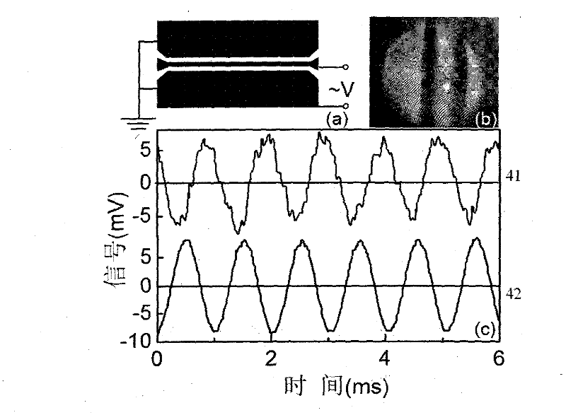
[0081] Example 3: Preparation of coplanar waveguides for electro-optical detection

[0082] A gold film with a thickness of 0.5 μm was prepared by thermal evaporation on K9 glass with a thickness of 2 mm and optical polishing on the upper and lower surfaces, with a size of 2 cm * 3 cm; The coplanar waveguide, whose structure is as image 3 (a) shown.

[0083] The electrical signal is fed into the center wire of the coplanar waveguide, and the electrical signal is provided by a signal generator (EM33151DDS full digital synthesis function signal generator), and the two sides of the center wire of the coplanar waveguide are ground wires. The coplanar waveguide is simulated as an integrated circuit in the experiment as the circuit 8 to be tested. The line width of the center wire is 100 μm, simulating the transmission line on the integrated circuit. The electrical signal on the center wire simulates the electrical signal on an actual integrated circuit.


PUM

PropertyMeasurementUnit
Thicknessaaaaaaaaaa
Thicknessaaaaaaaaaa
Thicknessaaaaaaaaaa

Abstract

The invention belongs to the integrated circuit fault diagnosis technology field, specifically relates to a novel electrooptical probe based on fluid electrooptical materials and a method of applying the electrooptical probe to detect a surface electric field of an integrated circuit. The electrooptical probe, along a direction of incident light, comprises a transparent substrate, a transparent conducting layer, a reflecting layer, an annular insulating layer, a fluid electrooptical material layer and a circuit to be measured. In the invention, fluid electrooptical materials are used as mediums to convert electrical signals to optical signals. On one hand, a problem of air gap existing between a traditional solid probe and the detected circuit can be avoided, therefore, losses in electrooptical transformation can be reduced and sensitivity of field measurement can be raised; on the other hand, because of a rotatable characteristic of electrooptical materials, the sensitivity of the field measurement can be substantially raised by an orientation effect of electrooptical molecules in the electric field. By using the probe and the method of the invention, a minimum measurable voltagecan reach a 10mV magnitude.

Description

technical field [0001] The invention belongs to the technical field of integrated circuit fault diagnosis, and in particular relates to a novel electro-optic probe based on fluid electro-optic material and a method for detecting the surface electric field of an integrated circuit by using the electro-optic probe. Background technique [0002] With the development of the integrated circuit manufacturing industry, the integration of chips is getting higher and higher, the operating speed is getting faster and faster, and the threshold voltage is getting lower and lower, which poses a severe challenge to integrated circuit testing, especially fault diagnosis. The fault diagnosis of integrated circuits is to find out the location or cause of the fault, so as to provide help for the design of integrated circuits and the improvement of manufacturing process. Therefore, fault diagnosis is of great significance to improve the reliability of integrated circuits, and has always been a...

Claims


Application Information

Patent Timeline
IPC IPC(8): G01R1/02G01R29/12
Inventor 孙洪波金如龙杨罕衣茂斌于颜豪
Owner 中科精仪科技(广东)有限公司
Learn More