

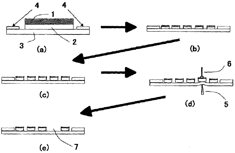
Method for processing wafer
A processing method and wafer technology, applied in the manufacturing of electrical components, electrical solid-state devices, semiconductor/solid-state devices, etc., can solve problems such as yield reduction, line speed, chip breakage, etc.
- Summary
- Abstract
- Description
- Claims
- Application Information
AI Technical Summary
Problems solved by technology
Method used
Image

Examples
Embodiment
[0278] The surface protection sheet for dicing used in the method of the present invention will be described in detail below based on examples, but the present invention is not limited to the use of the surface protection sheet for dicing of these examples. In addition, the shear elastic modulus of the elastic layer and the rigid film layer, and the adhesive force of the elastic layer to the shrinkable film were measured as follows. In addition, r / L, which is an index for judging whether or not it can function as a cylindrical wound body, is defined by the method shown below.
[0279] Determination of Young's modulus (80°C) of rigid film layer
[0280] The Young's modulus of the rigid film layer is measured by the following method in accordance with JIS K7127. As a tensile tester, Autograph AG-1kNG (with a heating mantle) manufactured by Shimadzu Corporation was used. A rigid film cut to a length of 200 mm×width of 10 mm was mounted at a chuck pitch of 100 mm. After formi...
manufacture example 1
[0292] Production of active energy ray-curable adhesive layer (1)
[0293] Acrylic acid-based polymer [composition: 2-ethylhexyl acrylate: morpholine acrylate: 2-hydroxyethyl acrylate = 75:25:22 (weight ratio) copolymerization] derived from 2-acrylic acid 50% of the hydroxyl group of hydroxyethyl ester is bonded with methacryloyloxyethyl isocyanate (2-isocyanatoethyl methacrylate) to produce an acrylic polymer with methacrylate group on the side chain .
[0294] 100 parts by weight of an acrylic polymer having a methacrylate group on the side chain, and 15 parts by weight of ARONIX M320 (manufactured by Toagosei Co., Ltd.; trimethylolpropane PO modified (n ≈ 2) triacrylate), and 1 part by weight of photoinitiator (manufactured by Ciba Geigy, trade name "IRGACURE 651"), and 1 part by weight of isocyanate-based crosslinking agent (trade name "CORONATE L" ) were mixed to prepare an active energy ray-curable adhesive.
[0295] The obtained active energy ray-curable adhesive w...
manufacture example 2
[0297] Production of inactive energy ray-curable adhesive layer (1)
[0298] 0.7 parts by weight of an epoxy-based crosslinking agent (manufactured by MITSUBISHI GAS CHEMICAL COMPANY, INC. name "TETRAD C"), and 2 parts by weight of an isocyanate-based crosslinking agent (trade name "CORONATE L") to prepare a non-active energy ray-curable adhesive.
[0299] Use an applicator to coat the obtained inactive energy ray-curable adhesive on a release sheet (manufactured by MITSUBISHI PLASTICS, INC., trade name "MRF38"), and then dry volatiles such as solvents to obtain A laminate of an inactive energy ray-curable pressure-sensitive adhesive layer having a thickness of 30 μm.
PUM
 Abstract
Description
Claims
Application Information