Substrate for flexible photoelectronic device and preparation method thereof

A technology of optoelectronic devices and substrates, which is applied in the fields of electrical solid-state devices, semiconductor/solid-state device manufacturing, and photovoltaic power generation, and can solve problems such as poor bonding force between silver nanowire films and flexible substrates, and large roughness of silver nanowire films

Inactive Publication Date: 2011-10-05
UNIV OF ELECTRONICS SCI & TECH OF CHINA
View PDF4 Cites 16 Cited by
  • Summary
  • Abstract
  • Description
  • Claims
  • Application Information

AI Technical Summary

Problems solved by technology

[0007] The problem to be solved by the present invention is: how to provide a substrate for flexible optoelectronic devices and its preparation method, the substrate solves the problems of large roughness of the silver nanowire film and poor bonding force between the silver nanowire film and the flexible substrate, Improve the electrical conductivity and surface smoothness of the silver nanowire film, and increase the bonding force between the silver nanowire film and the flexible substrate

Method used


Image

  • Substrate for flexible photoelectronic device and preparation method thereof
  • Substrate for flexible photoelectronic device and preparation method thereof
  • Substrate for flexible photoelectronic device and preparation method thereof

Examples


Embodiment 1

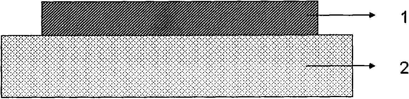
[0094] Such as figure 1 In the shown substrate structure, the flexible substrate 1 uses an adhesive that needs to be double-cured, and the conductive layer 2 uses a silver nanowire film, and the gaps of the silver nanowire film are filled with graphene.

[0095] The preparation method is as follows:

[0096] ① Clean the glass substrate with surface roughness less than 1nm, and dry it with dry nitrogen after cleaning;

[0097] ② Disperse the silver nanowires evenly in the solvent, and prepare the silver nanowire thin film on the clean substrate by spin coating. The rotation speed of the spin coating is 4000 rpm, the duration is 60 seconds, and the film thickness is about 70 nanometers;

[0098] ③ Drop-coat the graphene-containing solution on the silver nanowire film, place the glass substrate in an environment of 80°C for 30 minutes, remove the remaining solvent in the silver nanowire film, and then spray the double-cured adhesive on the silver nanowire film , the adhesive ra...

Embodiment 2

[0106] Such as figure 1 In the shown substrate structure, the flexible substrate 1 adopts an adhesive that requires double curing, the conductive layer 2 adopts a silver nanowire film, and the gaps of the silver nanowire film are filled with graphene, and the raw material of the adhesive includes the following components:

[0107]

[0108] The preparation method is similar to Example 1.

Embodiment 3

[0110] Such as figure 1 In the shown substrate structure, the flexible substrate 1 adopts an adhesive that requires double curing, the conductive layer 2 adopts a silver nanowire film, and the gaps of the silver nanowire film are filled with graphene, and the raw material of the adhesive includes the following components:

[0111]

[0112] The preparation method is similar to Example 1.


PUM

PropertyMeasurementUnit
surface roughnessaaaaaaaaaa

Abstract

The invention discloses a substrate for a flexible photoelectronic device. The substrate comprises a flexible substrate and a conducting layer, wherein the flexible substrate and the conducting layer are formed by one of the following two ways: (1) the flexible substrate is an adhesive needing dual-curing; the conducting layer is a silver nanowire film; and the gap of the silver nanowire film is filled with graphene; and (2) the flexible substrate is a graphene doped adhesive needing dual-curing; the conducting layer is a silver nanowire film; the gap of the silver nanowire film is filled with the graphene doped adhesive needing dual-curing; and the adhesive needing dual-curing comprises an ultraviolet curing-thermocuring system, an ultraviolet curing-microwave curing system, an ultraviolet curing-anaerobic curing system and an ultraviolet curing-electron beam curing system.

Description

technical field [0001] The invention relates to the technical field of organic optoelectronics, in particular to a substrate for a flexible optoelectronic device and a preparation method thereof. Background technique [0002] Optoelectronics technology is a rapidly developing industry with high technological content after microelectronics technology. With the rapid development of optoelectronic technology, optoelectronic products such as solar cells, optical image sensors, flat panel displays, and thin film transistors have gradually matured, and they have greatly improved people's lives. At the same time, the wide application of optoelectronic information technology in various fields of social life has also created a huge growing market. Developed countries regard the optoelectronic information industry as one of the key development areas, and the competition in the optoelectronic information field is unfolding worldwide. [0003] At present, organic optoelectronic device...

Claims


Application Information

Patent Timeline
Patent Type & Authority Applications(China)
IPC IPC(8): H01L51/44H01L51/46C09J167/06C09J4/00C09J163/00H01L51/48
CPCY02E10/549Y02E10/50
Inventor 于军胜于欣格黄江蒋亚东
Owner UNIV OF ELECTRONICS SCI & TECH OF CHINA
Why Eureka
Try Eureka