Method for preparing TiO2 (titanium dioxide) nano-pillar array on surface of LED (light-emitting diode) epitaxial wafer

A technology of LED epitaxial wafers and nano-column arrays, which is applied in the field of optoelectronics to achieve the effects of good uniformity, easy periodic arrays, and high controllability

Inactive Publication Date: 2011-10-12
SHANDONG UNIV
View PDF2 Cites 15 Cited by
  • Summary
  • Abstract
  • Description
  • Claims
  • Application Information

AI Technical Summary

Problems solved by technology

[0006] Aiming at the defects and problems existing in various methods for improving LED luminous efficiency, the present invention p

Method used


Image

  • Method for preparing TiO2 (titanium dioxide) nano-pillar array on surface of LED (light-emitting diode) epitaxial wafer
  • Method for preparing TiO2 (titanium dioxide) nano-pillar array on surface of LED (light-emitting diode) epitaxial wafer
  • Method for preparing TiO2 (titanium dioxide) nano-pillar array on surface of LED (light-emitting diode) epitaxial wafer

Examples


Embodiment 1

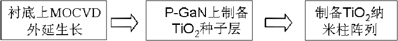
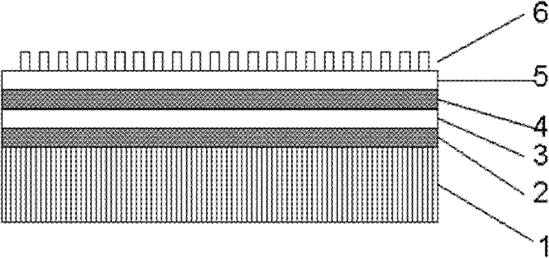
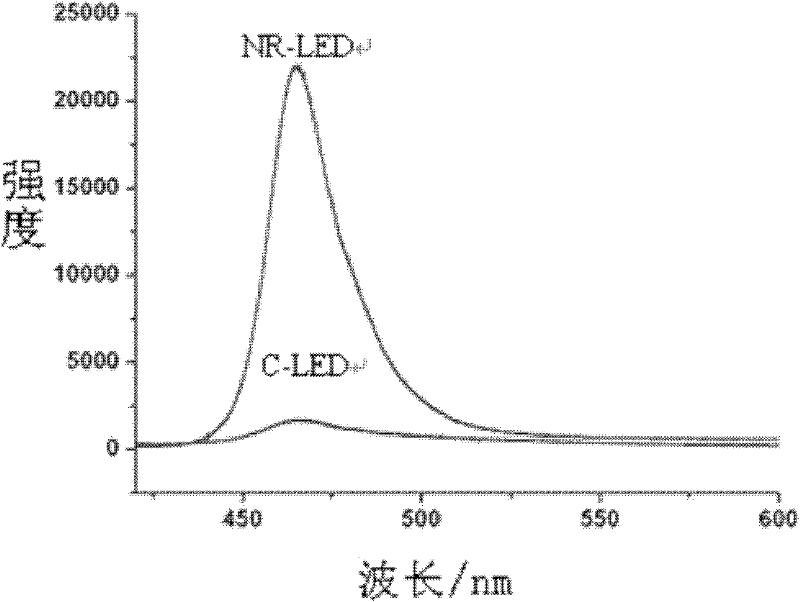
[0020] Such as figure 1 As shown, the present invention uses TiO 2 Nano-pillar arrays improve the photoluminescence efficiency of LED epitaxial wafers. The TiO 2 The preparation method of nanopillar array, because GaN has a hexagonal structure, TiO 2 It is a tetragonal structure, so first grow TiO on GaN 2 When arraying, you need to grow a seed layer. It includes the following steps:

[0021] (1) Using metal organic chemical vapor deposition (MOCVD) method to epitaxially grow N-type GaN layer 2, multiple quantum well active region 3 and P-type GaN layer 4 on sapphire substrate 1 to form epitaxial wafers;

[0022] (2) A layer of 50nm thick titanium is deposited on the surface of P-type GaN and calcined at 500℃ for 3 hours to transform the titanium into TiO 2 , Become TiO 2 As seed layer 5;

[0023] (3) Preparation of TiO by hydrothermal method 2 Nanopillar array 6, put 20mL of 4M HCl solution into the autoclave, stir for 5min at room temperature, add 1mL of tetrabutyl titanate, stir ...

Embodiment 2

[0027] The difference between this embodiment and embodiment 1 is:

[0028] In step (2), a layer of 1nm thick titanium is deposited on the surface of the P-type GaN layer and calcined at 400°C for 1 hour to convert the titanium to TiO 2 ;

[0029] In step (3), put 20 mL of 3M HCl solution into the autoclave, stir at room temperature for 1 min, add 1 mL of tetrabutyl titanate, and stir for 5 min to make a mixed solution; 2 The GaN substrate of the seed layer 5 was put into the mixed solution and leaned against the inner lining wall in a state inclined at 5 degrees to the horizontal plane, reacted at 120° C. for 24 hours, and cooled to room temperature.

Embodiment 3

[0031] The difference between this embodiment and embodiment 1 is:

[0032] In step (2), a layer of 200nm thick titanium is deposited on the surface of P-type GaN, and it is calcined at 600°C for 2 hours to convert the titanium to TiO 2 ;

[0033] In step (3), put 20 mL of 8M HCl solution in the autoclave, stir at room temperature for 10 minutes, add 5 mL of tetrabutyl titanate, and stir for 5 minutes to make a mixed solution; 2 The GaN substrate of the seed layer 5 is put into the mixed solution and leaned against the inner lining wall in an inclined state of 80 degrees with the horizontal plane, reacted at 150° C. for 1 hour, and cooled to room temperature.


PUM


Abstract

The invention discloses a method for preparing a TiO2 (titanium dioxide) nano-pillar array on a surface of an LED (light-emitting diode) epitaxial wafer. The method comprises the following steps: (1) preparing a GaN (gallium nitride) epitaxial wafer on a sapphire substrate; (2) evaporating a titanium layer on a surface of a P-type GaN layer of the epitaxial wafer, and carrying out calcination to transform titanium into TiO2 which is taken as a seeding layer; (3) adopting a hydrothermal method to prepare the TiO2 nano-pillar array, placing an HCl (hydrogen chloride) solution into an autoclave, stirring at a room temperature and adding tetrabutyl titanate to prepare a mixture solution; placing an epitaxial wafer with the TiO2 seedling layer into the mixture solution, leaning against a lining wall of the autoclave in a heeling condition, reacting for 1-24 hours at 120 DEG C-180 DEG C and cooling to the room temperature. The method is simple and practicable and has the advantages of low cost, high controllability, good homogenization and a periodical array is easy to form; in addition, the method can be utilized to improve the light-emitting efficiency of an LED, and the photoluminescence intensity of the LED can be improved by 7-8 times.

Description

Technical field [0001] The invention relates to a method for preparing titanium dioxide (TiO2) on the surface of an LED (light emitting diode) epitaxial wafer. 2 ) The method of nano-pillar array belongs to the field of optoelectronic technology. Background technique [0002] In the early 1990s, the third-generation wide-bandgap semiconductor materials represented by nitride made a historic breakthrough. Green, blue and purple LEDs were successfully fabricated on GaN-based materials, making LED white light illumination possible . With the continuous improvement of the performance of GaN-based LEDs, the luminous efficiency of white LEDs prepared with short-wavelength LEDs and phosphors has been greatly improved, and it is now recognized by the industry as the so-called green lighting that can replace traditional lighting lamps such as incandescent lamps and fluorescent lamps. light source. It has been widely used in landscape lighting, street lighting, indoor lighting, and speci...

Claims


Application Information

Patent Timeline
IPC IPC(8): H01L33/00H01L33/44B82Y40/00
Inventor 郝霄鹏刘晓燕吴拥中尹正茂周伟家徐现刚
Owner SHANDONG UNIV
Why Eureka
Try Eureka