

Preparation method for P-type CuAlO2 semiconductor material
A bulk material and semiconductor technology, applied in the field of preparation of CuAlO2 inorganic semiconductor bulk material, can solve problems such as adverse effects of materials, and achieve the effects of low pressure, simple process, and large output
- Summary
- Abstract
- Description
- Claims
- Application Information
AI Technical Summary
Problems solved by technology
Method used
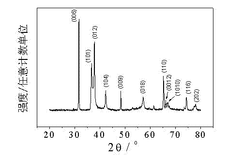
Image

Examples
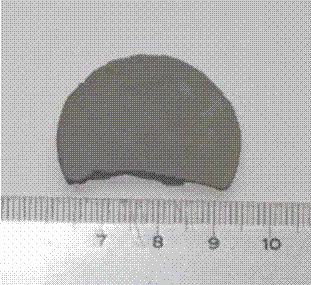
Embodiment 1
[0034] (1) Cu with a purity of 99.99% 2 O powder and Al with a purity of 99.999% 2 o 3 The powder is dosed at a molar ratio of 1:1, and then put into a ball mill jar for full grinding to obtain a uniformly mixed powder with a particle size not exceeding 300 nm.
[0035] (2) Using a powder tablet press, hold the pressure for 3 minutes under a static compression pressure of 30 MPa, and press the uniformly mixed powder into a cylindrical target blank with a diameter of about 3 cm and a height of 2 mm.
[0036] (3) Place the pressed target blank in the alumina ceramic boat, and then push the ceramic boat into the center of the alumina ceramic tube furnace. One end of the ceramic tube is connected to the argon gas cylinder through a set of sealing flanges and a vacuum pipeline with an inflation valve; the other end of the ceramic tube is connected to a vacuum pump through another set of sealing flanges and a vacuum pipeline with an air release valve .
[0037] (4) Turn on the v...
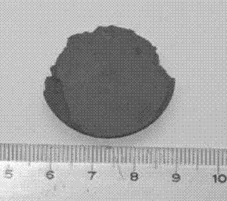
Embodiment 2
[0047] (1) Cu with a purity of 99.99% 2 O powder and Al with a purity of 99.999% 2 o 3 The powder is dosed at a molar ratio of 1:1, and then put into a ball mill jar for full grinding to obtain a uniformly mixed powder with a particle size not exceeding 300 nm.
[0048] (2) Using a powder tablet press, hold the pressure for 2 minutes under a static compression pressure of 30 MPa, and press the uniformly mixed powder into a cylindrical billet with a diameter of about 3 cm and a height of 4 mm.
[0049] (3) Place the pressed target blank in the alumina ceramic boat, and then push the ceramic boat into the center of the alumina ceramic tube furnace. One end of the ceramic tube is connected to the argon gas cylinder through a set of sealing flanges and a vacuum pipeline with an inflation valve; the other end of the ceramic tube is connected to a vacuum pump through another set of sealing flanges and a vacuum pipeline with an air release valve .
[0050] (4) Turn on the vacuum ...
PUM
| Property | Measurement | Unit |
|---|---|---|
| particle diameter | aaaaa | aaaaa |
Abstract
Description
Claims
Application Information