Crystalline silicon solar battery three-layer antireflection film and preparation method thereof
A technology of solar cells and anti-reflection coatings, applied in circuits, electrical components, semiconductor devices, etc., can solve the problems of low photoelectric conversion efficiency of solar cells, difficulty in achieving anti-reflection effects, low reflectivity of solar cells, etc., and achieve photoelectric conversion The effect of improving efficiency, improving photoelectric conversion efficiency, and simple preparation method
- Summary
- Abstract
- Description
- Claims
- Application Information
AI Technical Summary
Problems solved by technology
Method used
Image

Examples
Embodiment 1
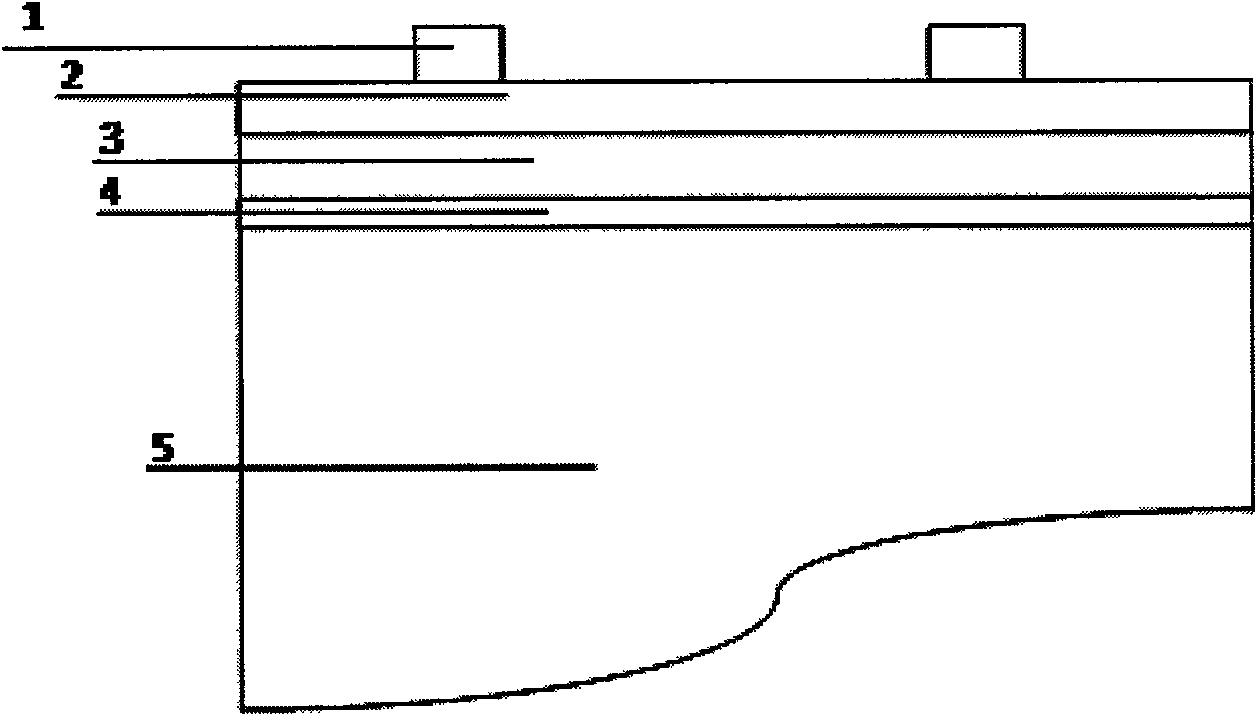
[0020] Example 1, such as figure 1 As shown, a three-layer anti-reflection film for a crystalline silicon solar cell is composed of three layers of films. The first layer is a silicon dioxide film 4 on the surface of a solar cell crystalline silicon 5 with a thickness of 20 nm and a refractive index of 1.15; The second layer is a titanium dioxide and silicon dioxide composite film 3 with a thickness of 80nm and a refractive index of 1.30; the third layer is a nano-titanium dioxide film 2 with a thickness of 50nm and a refractive index of 2.12. 1 is a grid line.
[0021] Anti-reflective coating is applied to the crystalline silicon wafers after the steps of cleaning and fabricating, diffusing to prepare PN junctions, etching and removing the PN junctions around the silicon wafer, and cleaning and removing the phosphosilicate glass, which includes the following steps:
[0022] 1. In the diffusion furnace, a layer of silicon dioxide film with a thickness of 20nm and a refractive ...
Embodiment 2
[0025] Example 2, such as figure 1 As shown, a three-layer anti-reflection film for a crystalline silicon solar cell is composed of three layers of films. The first layer is a silicon dioxide film 4 on the surface of a solar cell crystalline silicon 5 with a thickness of 30 nm and a refractive index of 1.25; The second layer is a titanium dioxide and silicon dioxide composite film 3 with a thickness of 90nm and a refractive index of 1.45; the third layer is a nano-titanium dioxide film 2 with a thickness of 60nm and a refractive index of 2.28. 1 is a grid line.
[0026] Coating anti-reflection film on the crystalline silicon wafer after cleaning and making texture, diffusing to prepare PN junction, etching and removing the PN junction around the crystalline silicon wafer, cleaning and removing the phosphosilicate glass, comprises the following steps:
[0027] 1. In the diffusion furnace, a layer of silicon dioxide film with a thickness of 30nm and a refractive index of 1.25 is...
Embodiment 3
[0030] Example 3, such as figure 1 As shown, a three-layer anti-reflection film for a crystalline silicon solar cell is composed of three layers of films. The first layer is a silicon dioxide film 4 on the surface of a solar cell crystalline silicon 5 with a thickness of 23nm and a refractive index of 1.18; The second layer is a titanium dioxide and silicon dioxide composite film 3 with a thickness of 85nm and a refractive index of 1.4; the third layer is a nano-titanium dioxide film 2 with a thickness of 55nm and a refractive index of 2.15. 1 is a grid line.
[0031] Anti-reflective coating is applied to the crystalline silicon wafers after the steps of cleaning and fabricating, diffusing to prepare PN junctions, etching and removing the PN junctions around the silicon wafer, and cleaning and removing the phosphosilicate glass, which includes the following steps:
[0032] 1. In the diffusion furnace, a silicon dioxide film with a thickness of 23nm and a refractive index of 1....
PUM
| Property | Measurement | Unit |
|---|---|---|
| thickness | aaaaa | aaaaa |
| thickness | aaaaa | aaaaa |
| thickness | aaaaa | aaaaa |
Abstract
Description
Claims
Application Information
 - R&D
- Intellectual Property
- Life Sciences
- Materials
- Tech Scout
- Unparalleled Data Quality
- Higher Quality Content
- 60% Fewer Hallucinations
Browse by: Latest US Patents, China's latest patents, Technical Efficacy Thesaurus, Application Domain, Technology Topic, Popular Technical Reports.
© 2025 PatSnap. All rights reserved.Legal|Privacy policy|Modern Slavery Act Transparency Statement|Sitemap|About US| Contact US: help@patsnap.com