Integrated circuit element and forming method of bumping block structure

A technology of integrated circuits and components, applied in the field of bump structure, can solve the problems of high manufacturing cost, interface delamination, solder wetting to the sidewall, etc., to overcome Ni protrusion, increase adhesion, and save process costs.

Active Publication Date: 2011-11-09
TAIWAN SEMICON MFG CO LTD
View PDF3 Cites 30 Cited by
  • Summary
  • Abstract
  • Description
  • Claims
  • Application Information

AI Technical Summary

Problems solved by technology

Therefore, a sidewall protection layer is needed to avoid copper oxidation, but the traditional method of treating the sidewall of copper pillars requires high manufacturing costs and has interface delamination problems
At present, the chemical immersion tin process (immersion tin process) is used to provide a tin layer on the sidewall of the copper pillar, but there are still problems of manufacturing cost, adhesion between tin and underfill, and solder wetting to the sidewall. It is a challenge for the fine-pitch packaging technology of the new generation of chips

Method used


Image

  • Integrated circuit element and forming method of bumping block structure
  • Integrated circuit element and forming method of bumping block structure
  • Integrated circuit element and forming method of bumping block structure

Examples


Embodiment Construction

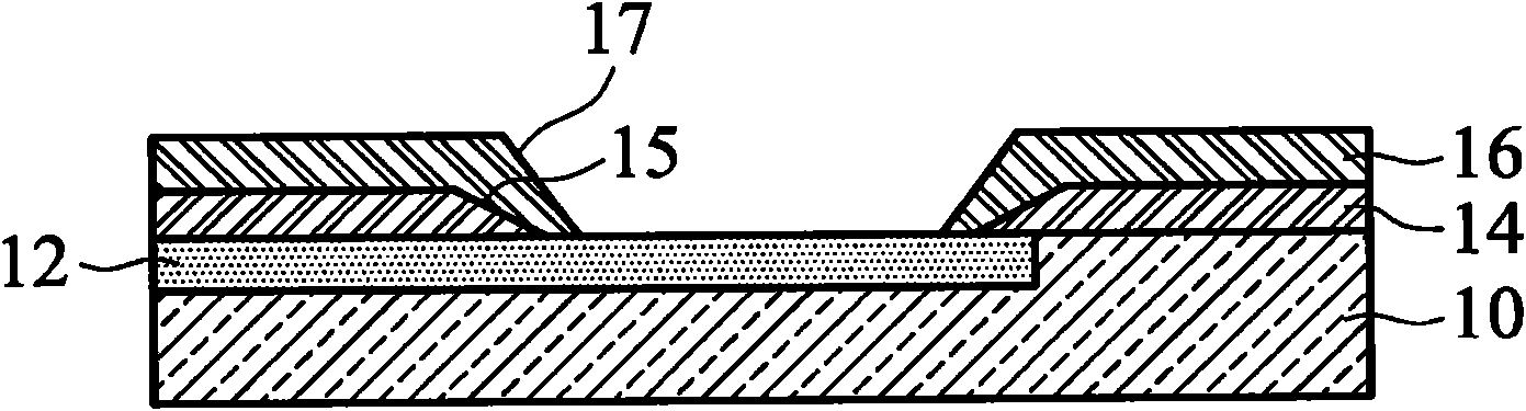
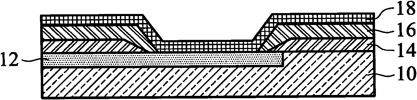
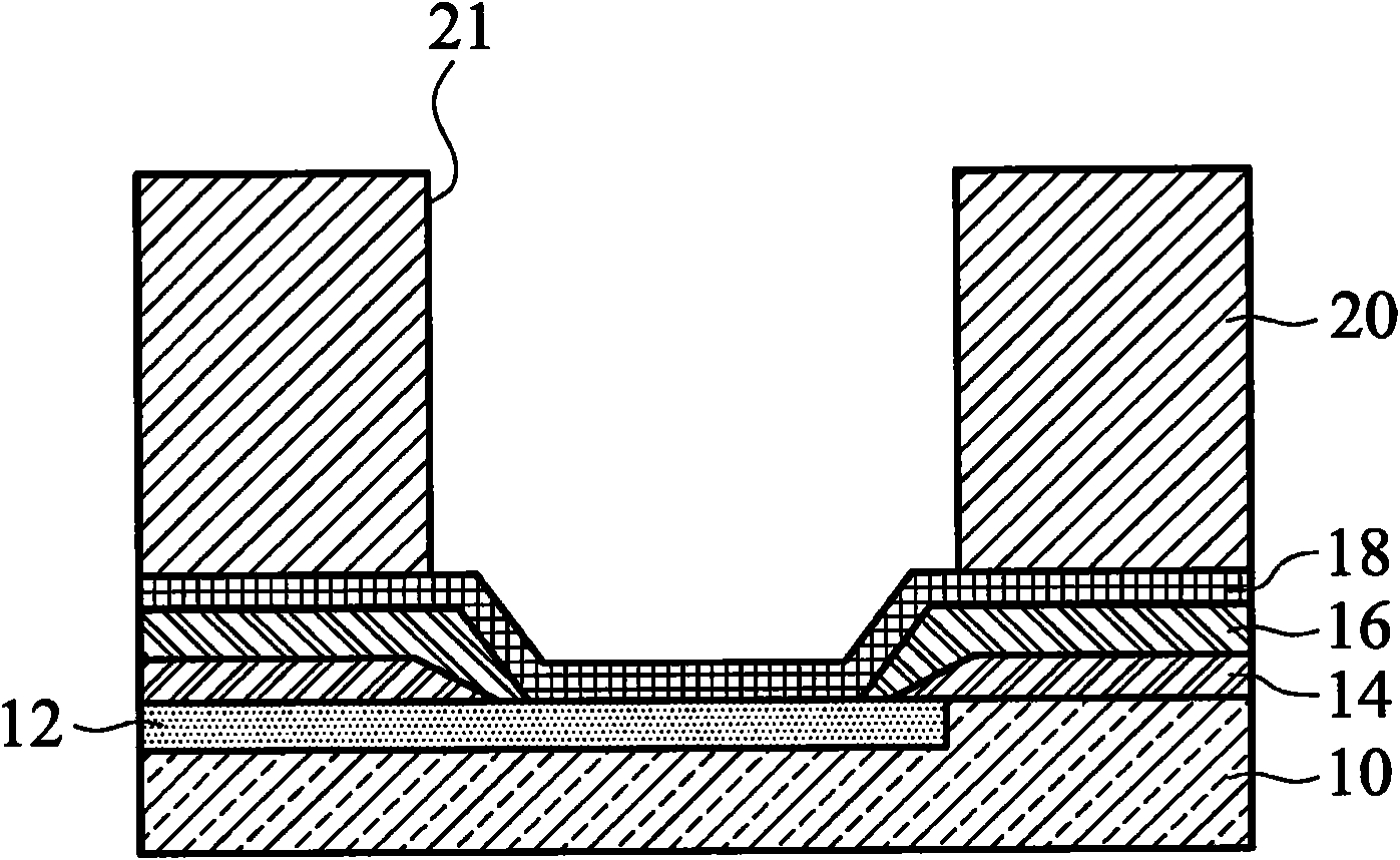
[0014] Embodiments disclosed herein provide a sidewall protection process for copper pillar bump technology, wherein the protection layer on the sidewall of the copper pillar bump is a metal layer formed by an electrolytic process, also referred to herein as electrolytic metal Floor. Copper pillar bumps can be used directly on conductive pads or redistribution layers of semiconductor chips, and can also be used for flip chip assembly or other similar applications.

[0015] In the embodiments of the present invention, the present invention is described in detail with reference to the drawings. As shown in the drawings, the same reference numerals are used as much as possible in the drawings and descriptions to indicate the same or similar parts. In the drawings, the shapes and thicknesses of the embodiments may be exaggerated for the purpose of convenient description and clear display. The description of the specification relates directly to some elements of a device formed in...


PUM


Abstract

The invention provides an integrated circuit element and a forming method of a bumping block structure. The integrated circuit element comprises a semiconductor substrate, a bumping block metal layer disposed on the semiconductor substrate, a copper column which is disposed on the bumping block lower metal layer and has a side wall surface and an upper surface, and a protection layer which is disposed on the side wall surface and the upper surface of the copper column. The protection layer is a nickel-containing layer, including phosphor with content being less than 0.01 weight%. The invention provides a copper column bumping block, having a side wall protection layer formed by an electrolytic metal layer. The electrolytic metal layer is an electrolytic nickel layer, an electrolytic gold layer, an electrolytic copper layer or an electrolytic silver layer, preventing the copper column side wall from oxidation, and increasing the adhesion strength between the copper column side wall and the bottom filler materials formed afterwards. The bumping block can prevent stress to be concentrated on one point, resolving the problem that the bumping blocks are peeled off or delaminated from the copper column side wall.

Description

technical field [0001] The present invention relates to the manufacture of integrated circuits, and more particularly to bump structures for integrated circuit components. Background technique [0002] Modern integrated circuits are formed of millions of active elements, such as transistors and capacitors, that are initially isolated from each other but are later interconnected to form a functional circuit. A typical interconnection structure includes horizontal interconnections, such as metal lines (wires), and vertical interconnections, such as vias and contacts. Interconnects are increasingly limiting the density and performance of modern integrated circuits. Influence. The bonding pad is formed on the top of the interconnect structure and is exposed on the surface of the individual chip. The bonding pad can form an electrical connection connecting the chip to the package substrate or other die. The bonding pad Can be used for wire bonding or flip chip bonding. [0003...

Claims


Application Information

Patent Timeline
Patent Type & Authority Applications(China)
IPC IPC(8): H01L23/00H01L21/60
CPCH01L2924/01006H01L2224/13455H01L24/11H01L2224/13644H01L2924/00013H01L2224/11825H01L2224/0346H01L2924/01038H01L2924/01012H01L2924/0001H01L2224/13647H01L2924/01022H01L2924/01047H01L2224/13082H01L2924/01079H01L2224/11823H01L24/13H01L2924/01013H01L2924/01078H01L24/03H01L2224/03912H01L2224/1357H01L2924/01049H01L2924/01327H01L2924/01082H01L2924/01046H01L2224/13022H01L2224/13565H01L2924/04941H01L2224/11462H01L2224/11906H01L2924/01073H01L2224/05572H01L2224/11452H01L2924/01019H01L2224/13083H01L2924/13091H01L2924/014H01L2224/13099H01L2924/01025H01L2224/13655H01L2224/13639H01L2224/1147H01L2924/01023H01L2924/01032H01L2224/13147H01L2924/19041H01L2924/01029H01L2924/01024H01L2924/0104H01L24/05H01L2924/0103H01L2924/1306H01L2924/1305H01L2924/00014H01L2924/0002H01L2224/0401H01L2924/14H01L2224/0361H01L2224/1308H01L2224/13599H01L2224/05599H01L2224/05099H01L2224/29099H01L2224/29599H01L2924/00H01L2224/05552
Inventor 吕文雄郑明达林志伟张俊华刘重希余振华
Owner TAIWAN SEMICON MFG CO LTD
Why Eureka
Try Eureka