
Method of growing silicon-based gallium arsenide material with inverted V-shaped silicon dioxide groove structure

A silicon-based gallium arsenide and silicon dioxide technology, applied in electrical components, semiconductor/solid-state device manufacturing, circuits, etc., can solve problems that affect the quality of epitaxial layers, and achieve the effects of reducing defects, improving quality, and reducing growth temperature

Active Publication Date: 2013-02-06
INST OF SEMICONDUCTORS - CHINESE ACAD OF SCI
View PDF3 Cites 0 Cited by
  • Summary
  • Abstract
  • Description
  • Claims
  • Application Information

AI Technical Summary

Problems solved by technology

These dislocations and antiphase domain boundaries will extend all the way to the surface of the epitaxial layer, seriously affecting the quality of the epitaxial layer

Method used


Image

  • Method of growing silicon-based gallium arsenide material with inverted V-shaped silicon dioxide groove structure
  • Method of growing silicon-based gallium arsenide material with inverted V-shaped silicon dioxide groove structure
  • Method of growing silicon-based gallium arsenide material with inverted V-shaped silicon dioxide groove structure

Examples


Embodiment Construction

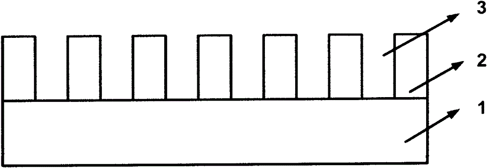
[0031] see Figure 1 to Figure 6 , a method for growing silicon-based gallium arsenide material in an inverted V-shaped silicon dioxide trench structure of the present invention, comprising the following steps:

[0032] Step 1: growing a silicon dioxide layer 2 on a silicon substrate 1 ( figure 1 Middle), the silicon substrate 1 is high-resistance (001) silicon with a p-type resistivity greater than 2000Ωcm, and the thickness of the silicon dioxide layer 2 is 500nm-1000nm;

[0033] Step 2: using conventional photolithography and RIE methods to etch a plurality of trenches 3 on the silicon dioxide layer 2 along the direction of the silicon substrate 1 ( figure 2 In), the width of the groove 3 is 200-300nm;

[0034] Step 3: using silane as a raw material to form an inverted V-shaped silicon buffer layer 4 ( image 3 Middle), the distance between its apex and the silicon substrate 1 is 100nm-200nm;

[0035] Step 4: Use piranha and SC respectively 2 , HF and deionized water...


PUM


Abstract

The invention relates to a method of growing a silicon-based gallium arsenide material with an inverted V-shaped silicon dioxide groove structure, which comprises the following steps of: 1. growing a silicon dioxide layer on a silicon substrate; 2. etching a groove on the silicon dioxide layer along the direction of the silicon substrate (110) by using a traditional photoetching and RIE (ReactiveIon Etching) method, wherein the etching thickness is equal to the thickness of the silicon dioxide layer; 3. etching an inverted V-shaped silicon buffer layer formed on the silicon substrate in the groove by using silicane as a raw material and adopting a VPE (Vapor Phase Epitaxy) method; 4. cleaning the silicon buffer layer at the bottom of the groove by using piranha, SC2 and HF (Hydrogen Fluoride) and deionized water respectively; 5. by adopting a low pressure MOCVD (Metal-organic Chemical Vapor Deposition) method, firstly, growing a GaAs buffer layer in the groove, then growing a GaAs top layer on the GaAs buffer layer in the groove; and 6. by adopting a chemical mechanical polishing method, polishing the GaAs top layer exceeding the groove till the GaAs top layer is flush with the silicon dioxide layer, and finishing the preparation of the silicon-based gallium arsenide material.

Description

technical field [0001] The present invention relates to the field of semiconductor technology, and combines MOCVD, high aspect ratio trench confinement technology (Aspect Ratio Trapping, ART) and inverted V-shaped grooves to grow silicon-based gallium arsenide materials applied to nMOS, in particular to a A method for growing silicon-based gallium arsenide material with an inverted V-shaped silicon dioxide trench structure. Background technique [0002] According to the forecast of the International Semiconductor Industry Technology Development Blueprint (ITRS2009), the physical gate length of the MPU will be reduced to 22 nanometers in 2012. However, with the development of integrated circuit technology to the 22nm technology node and below, silicon integrated circuit technology will be limited by a series of basic physical problems and process technology problems in terms of speed, power consumption, integration, reliability, etc., and expensive High production line const...

Claims


Application Information

Patent Timeline
Patent Type & Authority Patents(China)
IPC IPC(8): H01L21/205H01L21/336
Inventor 周旭亮于红艳王宝军潘教青王圩
Owner INST OF SEMICONDUCTORS - CHINESE ACAD OF SCI
Learn More