
Method for growing Gaas material hemt device in art structure trench

An in-growth and trench technology, applied in semiconductor/solid-state device manufacturing, electrical components, circuits, etc., can solve problems affecting the quality of epitaxial layers, and achieve the effect of reducing defects, improving device quality, and improving quality

Active Publication Date: 2016-01-13
INST OF SEMICONDUCTORS - CHINESE ACAD OF SCI
View PDF5 Cites 0 Cited by
  • Summary
  • Abstract
  • Description
  • Claims
  • Application Information

AI Technical Summary

Problems solved by technology

These dislocations and antiphase domain boundaries will extend all the way to the surface of the epitaxial layer, seriously affecting the quality of the epitaxial layer

Method used


Image

  • Method for growing Gaas material hemt device in art structure trench
  • Method for growing Gaas material hemt device in art structure trench
  • Method for growing Gaas material hemt device in art structure trench

Examples


Embodiment Construction

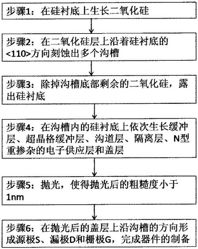
[0019] see figure 1 , and see Figure 2 to Figure 7 The present invention provides a method for growing a GaAs material HEMT device in an ART structure trench, comprising the following steps:

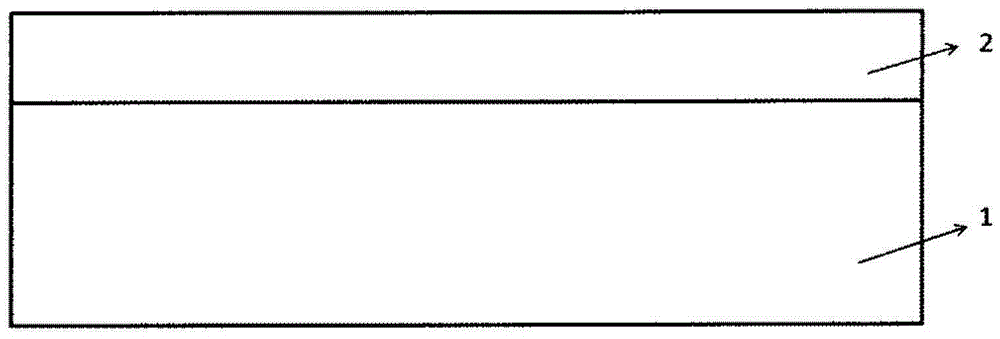
[0020] Step 1: grow silicon dioxide layer 2 on silicon substrate 1 (see figure 2 ), the thickness of the silicon dioxide layer 2 is 600-700nm, and the preferred thickness is 600nm; when growing, we choose a Si substrate with a certain off angle (6°-7°), which can limit the antiphase domain ( APD) formation. At the same time, using high aspect ratio confinement technology, using SiO with AR>1 2 Trench to better confine fitting dislocations and APD formation.

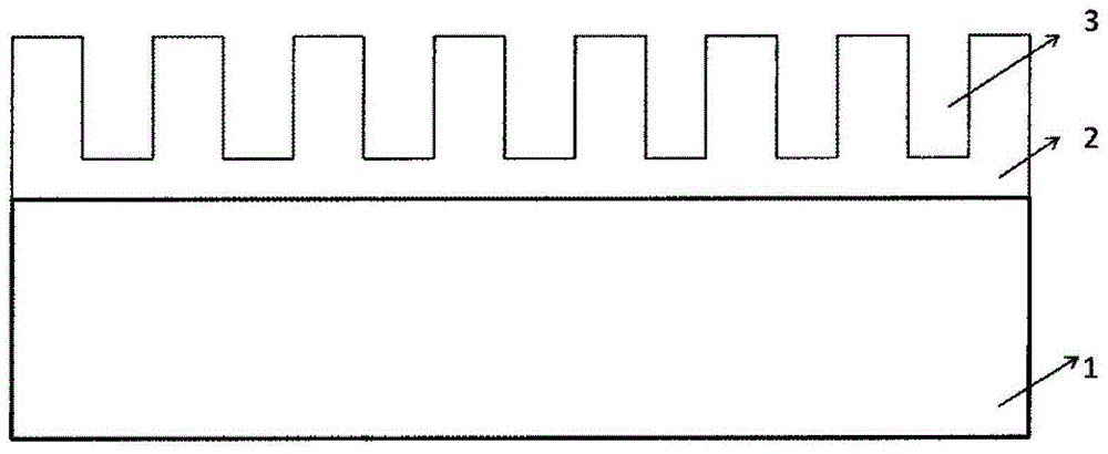
[0021] Step 2: Etch a plurality of trenches 3 along the direction of the silicon substrate 1 on the silicon dioxide layer 2 by holographic exposure and ICP (see image 3 ), the width of the trench 3 is 200-300nm, and the depth is the same as the thickness of the silicon dioxide layer 2; in SiO 2 In the trench, epitaxial GaA...


PUM


Abstract

The invention discloses a method of growing a high electron mobility transistor (HEMT) device of GaAs materials in an ART-structure groove. The method comprises the following steps. A silica layer is grown on a silicon substrate, and a plurality of grooves are etched on the silica layer along the direction of the silicon substrate (110) through holographic exposure and an inductively coupled plasma (CIP) method. Piranha, SC2, HF and deionized water are respectively used for cleaning. The rest silica layer at the bottoms of the grooves is removed, and the silicon substrate is exposed. A metal organic chemical vapor deposition (MOCVD) method is utilized so that a buffering layer, a superlattice buffering layer, a channel layer, an isolating layer, an N-shaped heavy doping electronic supplying layer and a cover layer are sequentially and slowly grown on the silicon substrate in the grooves. A chemical polishing method is utilized for polishing the cover layer, and roughness of the cover layer after polishing is less than 1nm. By the crafts of photoetching, corrosion and metal wiring, a source electrode, a drain electrode and a grid electrode are formed on the cover layer after the cover layer is polished along the direction of the grooves, and manufacture of the device is finished. By changing raw materials, adding the superlattice buffering layer and combining high aspect ratio groove limiting technology, adaptive dislocation of an interface and extension to an outer layer of amplitude probability distribution (APD) are restrained.

Description

technical field [0001] The invention relates to a method combining MOCVD and a high aspect ratio trench confinement technology (AspectRatioTrapping, ART), in particular to a method for growing a GaAs material HEMT device in a trench with an ART structure. Background technique [0002] According to the forecast of the International Semiconductor Industry Technology Development Blueprint (ITRS2009), the physical gate length of the MPU will be reduced to 22 nanometers in 2012. However, with the development of integrated circuit technology below the 22nm technology node, silicon integrated circuit technology is limited by a series of basic physical problems and process technology in terms of speed, power consumption, integration, reliability, etc., and expensive production lines Construction and manufacturing costs make the integrated circuit industry face huge investment risks, and the traditional silicon CMOS technology adopts "downscaling" to achieve smaller, faster, and chea...

Claims


Application Information

Patent Timeline
Patent Type & Authority Patents(China)
IPC IPC(8): H01L21/335H01L21/205
Inventor 李梦珂周旭亮于红艳李士颜米俊萍潘教青
Owner INST OF SEMICONDUCTORS - CHINESE ACAD OF SCI
Learn More