Monocrystalline silicon with photoluminescent characteristics and preparation method thereof

A photoluminescence and single crystal silicon technology, applied in the directions of luminescent materials, chemical instruments and methods, can solve the problems of reduced luminous efficiency, destruction, and no luminescence of devices, and achieves simple preparation method, wide application prospect and high luminous efficiency. Effect

Inactive Publication Date: 2013-10-23
JIANGSU UNIV
View PDF1 Cites 0 Cited by
  • Summary
  • Abstract
  • Description
  • Claims
  • Application Information

AI Technical Summary

Problems solved by technology

[0005] In the prior art, porous silicon prepared by different methods has luminescent properties, but it is generally believed that the chemical properties of porous silicon prepared by chemical methods such as electrochemical deposition, chemical polymerization, sol-gel and chemical vapor deposition are unstable. The silicon-hydrogen bond on its surface is very weak, and it is easy to be destroyed to form dangling bonds. The dangling bonds will cause non-radiative recombination of electron-hole pairs in photosensitive devices, resulting in a decrease in luminous efficiency, and even non-luminous and non-luminescent devices. failure, etc., there are many problems in the specific application environment

Method used


Image

  • Monocrystalline silicon with photoluminescent characteristics and preparation method thereof
  • Monocrystalline silicon with photoluminescent characteristics and preparation method thereof
  • Monocrystalline silicon with photoluminescent characteristics and preparation method thereof

Examples


Embodiment 1

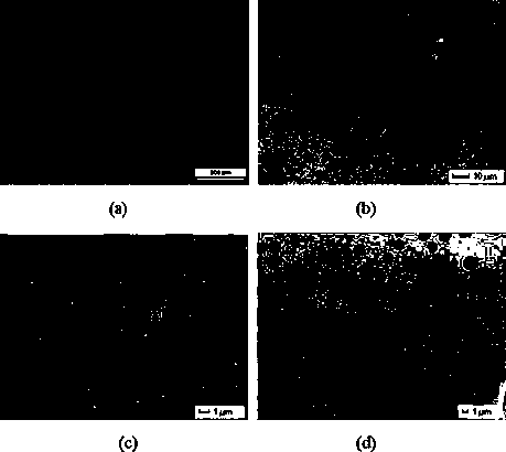
[0031] Using oriented monocrystalline silicon wafer as raw material, its resistivity ρ=1~20Ω / m, thickness T=490±10μm, such as figure 1 Shown is the optical micrograph of the polished surface of single crystal silicon before HCPEB bombardment. The polished surface was used as the bombarded surface during the preparation process. It can be seen from the figure that the surface to be bombarded is smooth and basically free of impurities.

[0032] Use Gatan601 type ultrasonic to cut the above-mentioned single crystal silicon wafer into test samples with a size of 2cm×1cm, put the test samples in alcohol-acetone solution (1:1) and ultrasonically clean them for 10min, take them out and dry them with nitrogen before use. The above cleaned and dried single crystal silicon sample is placed in an electron beam emission device, and the surface of the single crystal silicon is subjected to electron beam pulse bombardment treatment. During the pulse bombardment treatment on the surface of t...

Embodiment 2

[0038]Using oriented single crystal silicon wafer as raw material, its resistivity ρ=30~50Ω / m, thickness T=500±10μm, the above single crystal silicon wafer is cut into 2cm×1cm size by Gatan601 ultrasonic wave For the test sample, place the test sample in an alcohol-acetone solution (1:1) and ultrasonically clean it for 10 minutes, take it out and blow it dry with nitrogen before use, and place the single crystal silicon sample after the above cleaning and drying in the electron beam emission device. Electron beam pulse bombardment treatment is performed on the surface of single crystal silicon.

[0039] In the pulse bombardment treatment of the surface of a single crystal silicon sample, the electron beam energy of the HCPEB emission device is 21.6~27KeV, the number of bombardments is 1~30, and the vacuum degree P≤8×10 -3 Pa, the distance L=6cm between the single crystal silicon sample and the cathode electron gun.

[0040] The photoluminescence (PL) characteristics of the ...


PUM

PropertyMeasurementUnit
wavelengthaaaaaaaaaa
electrical resistivityaaaaaaaaaa
thicknessaaaaaaaaaa

Abstract

The invention belongs to the field of the preparation of raw materials of light-emitting semiconductors, and particularly relates to monocrystalline silicon with photoluminescent characteristics and a preparation method thereof. The wavelength of a luminescent spectrum of the monocrystalline silicon is 380 to 420nm. The preparation method comprises the following steps of: cleaning monocrystallinesilicon, and blow-drying for later use; and putting the monocrystalline silicon into an electron beam emitting device, and performing pulse bombardment on the surface of the monocrystalline silicon to obtain the monocrystalline silicon with photoluminescent characteristics. In the invention, the monocrystalline silicon with photoluminescent characteristics has a stable structure, high luminous efficiency and long attenuation time; and as a novel light-emitting semiconductor material, the monocrystalline silicon with photoluminescent characteristics has broad application prospect.

Description

technical field [0001] The invention belongs to the field of preparation of light-emitting semiconductor raw materials, and in particular relates to a single crystal silicon with photoluminescent properties and a preparation method thereof. Background technique [0002] As we all know, the semiconductor material silicon occupies an important position in the semiconductor industry due to its unique properties. Silicon element has the characteristics of high thermal conductivity, small expansion coefficient and high yield strength, so it is easy to stretch into larger single crystals. Crystal silicon is used as the raw material, and microelectronics technology with VLSI as the main body has been highly developed. It is an inevitable development to replace electrons with light as the carrier of information to meet the requirements of faster information processing, larger storage capacity, and stronger processing capabilities. Trend, single crystal silicon is the main material o...

Claims


Application Information

Patent Timeline
Patent Type & Authority Patents(China)
IPC IPC(8): C09K11/59
Inventor 关庆丰彭冬晋李艳顾倩倩
Owner JIANGSU UNIV
Why Eureka
Try Eureka