A kind of magnetic nanometer multilayer film for magnetic sensor and its manufacturing method
A magnetic sensor, magnetic nanotechnology, applied in the nanotechnology for information processing, the manufacture/processing of electromagnetic devices, the size/direction of the magnetic field, etc. Device miniaturization and other issues, to achieve the effect of easy microfabrication, preparation and integration, and low process difficulty
- Summary
- Abstract
- Description
- Claims
- Application Information
AI Technical Summary
Problems solved by technology
Method used
Image
Examples
example 1
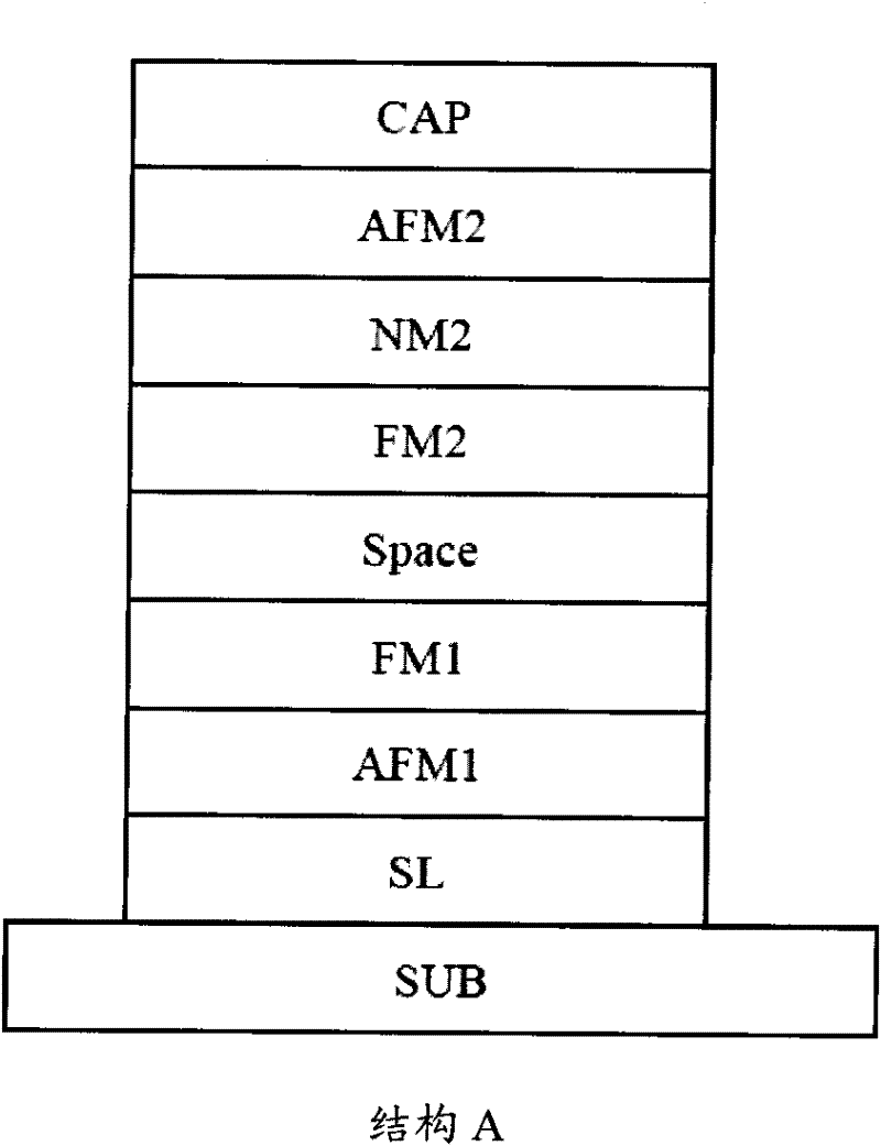
[0081] 1) Choose a Si-SiO with a thickness of 1mm 2 The substrate is used as the substrate SUB, and the vacuum on the magnetron sputtering equipment is better than 2×10 -6 Pa, the deposition rate is 0.1nm / s, and the argon pressure during deposition is the condition of 0.07Pa, the seed layer SL of Ta(5nm) / Ru(20nm) / Ta(5nm) is deposited on the substrate;
[0082] 2) On the magnetron sputtering equipment, the vacuum is better than 2×10 -6 Pa, the deposition rate is 0.1nm / s, and the argon pressure is 0.07Pa, and the first antiferromagnetic layer AF1 with a thickness of 15nm of IrMn is deposited on the seed layer SL;
[0083] 3) On the magnetron sputtering equipment, the vacuum is better than 2×10 -6 Pa, under the condition that the deposition rate is 0.06nm / s, and the argon pressure is 0.07Pa, the first ferromagnetic layer FM1 of CoFeB with a thickness of 2.5nm is deposited on the first antiferromagnetic layer AF1;
[0084] 4) On the magnetron sputtering equipment, the vacuum is...
example 2~6
[0094] Prepare Examples 2-6 according to the method of Example 1, the difference lies in the composition and thickness of each layer (as shown in Table 1 below), and the two annealing temperatures are based on the Bloch of the two antiferromagnetic layers in the reference layer and the detection layer The temperature is properly determined.
[0095] Table 1
[0096]
[0097] (Unless marked, the thickness units in the list are in nanometers)
[0098] The device resistance of the magnetic tunnel junctions of Examples 2-6 and the external magnetic field are tested, and the results show that the magnetoresistance response curves of Examples 2-6 all present a linear response to an external magnetic field.
example 7~11
[0100] Examples 7-11 are prepared in a method similar to Example 1, except that the magnetic nano-multilayer film of Examples 7-11 is structure B, that is: SUB / SL / AFM1 / FM1 / Space / FM2(1) / NM2 / FM2(2) / AFM2 / CAP, such as Figure 5 As shown, the composition and thickness of each layer are shown in Table 2 below.
[0101] Table 2
[0102]
[0103]
[0104] (Unless marked, the thickness units in the list are in nanometers)
[0105] The device resistance and the external magnetic field of the magnetic tunnel junctions of Examples 7-11 above were tested, and the results showed that the magnetoresistance response curves of Examples 7-11 all showed a linear response to the external magnetic field.
PUM
 Abstract
Description
Claims
Application Information


