A Fabrication Method of Microcantilever Probe Based on (110) Single Crystal Silicon

A technology of micro-cantilever beam and manufacturing method, which is applied in the field of MEMS and testing, can solve the problem that the taper of the needle tip is not easy to control, and achieve the effect of low cost and good optical surface

Inactive Publication Date: 2011-12-14
DALIAN UNIV OF TECH
View PDF7 Cites 11 Cited by
  • Summary
  • Abstract
  • Description
  • Claims
  • Application Information

AI Technical Summary

Problems solved by technology

It overcomes the problems of interference between the needle tip and the reticle in the traditional micro-cantilever beam probe manufacturing process, and the

Method used


Image

  • A Fabrication Method of Microcantilever Probe Based on (110) Single Crystal Silicon
  • A Fabrication Method of Microcantilever Probe Based on (110) Single Crystal Silicon
  • A Fabrication Method of Microcantilever Probe Based on (110) Single Crystal Silicon

Examples


Embodiment 1

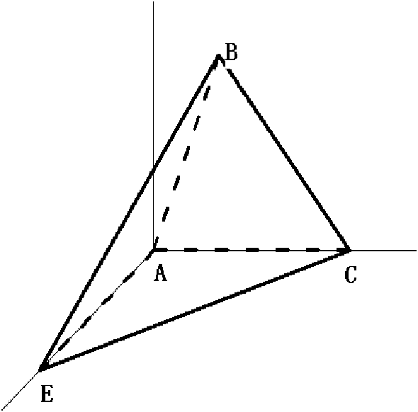
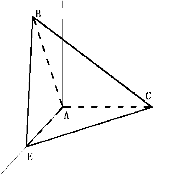
[0047] For the silicon nitride micro-cantilever probe manufactured in this embodiment, the length of the micro-cantilever is 450 microns, the width is 70 microns, and the tip height is 5 microns. A micro-cantilever beam probe was fabricated using an N-type (110) double-sided polished single-crystal silicon wafer with a thickness of 310 microns as the substrate.

[0048] Its specific production process is as follows:

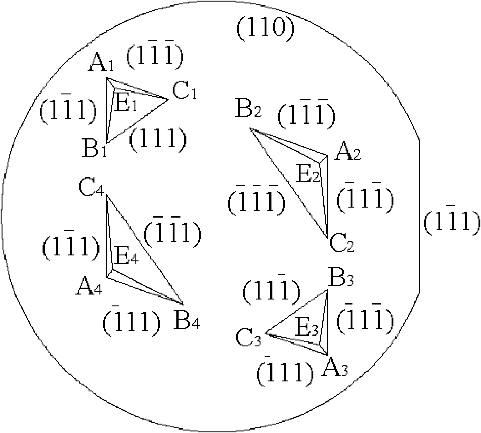
[0049] ①Conventional thermal oxidation of single crystal silicon wafer 1, forming upper surface silicon dioxide layer 2 and lower surface silicon dioxide layer 3 on the single crystal silicon wafer, the thickness of the oxide layer is about 1 micron, as attached Figure 3a .

[0050] ②Silicon wafer backside treatment process: backside photolithography, and use hydrofluoric acid buffer solution (BHF) to etch silicon dioxide to produce a rectangular window pattern 3′ with silicon dioxide removed, as shown in the attached Figure 4a , so that silicon is exposed to...


PUM


Abstract

The invention discloses a method for manufacturing a micro cantilever probe based on monocrystalline silicon (110), which belongs to the technical fields of micro-electro-mechanical systems (MEMS) and tests and is characterized by using a process of manufacturing the pinpoint of a silicon nitride micro cantilever probe based on the monocrystalline silicon (110). In the manufacturing process, the anisotropic corrosion self-stopping method of the monocrystalline silicon (110) is used. The method for manufacturing the micro cantilever probe based on the monocrystalline silicon (110) has the advantages that: a complete process flow can be accomplished by an MEMS processing technique, the influence of the anisotropic corrosion solution of the common monocrystalline silicon on the surface roughness of the monocrystalline silicon (110) is eliminated, the requirement on process equipment is low, and the micro cantilever probe can be produced in batches, so that product cost is lowered. The pinpoint of the silicon nitride nano-probe manufactured by the method has the advantages of very normative shape, high hardness, high abrasive resistance and the like. The cantilever probe manufactured by the method can be applied to an atomic force microscope (AFM) probe, a high-density memory device probe and a micro nano-processing device.

Description

technical field [0001] The invention belongs to the technical field of MEMS and testing, and relates to a manufacturing method of a micro-cantilever beam probe, which is suitable for an atomic force microscope (AFM) probe, a high-density storage device probe and a micro-nano processing device. Background technique [0002] Atomic force microscope (AFM) is a high-definition surface analyzer. This surface analysis instrument observes the surface structure of the sample by detecting the change of the weak interatomic force between the needle tip and the sample surface. AFM can not only observe the surface morphology of conductive materials, but also observe the surface morphology of non-conductive materials. Therefore, it has become a powerful tool for humans to observe and study the microscopic world. The traditional AFM is mainly a laser detection-like atomic force microscope. The key part is a force sensor composed of a micro-cantilever beam and a probe at the end of the b...

Claims


Application Information

Patent Timeline
IPC IPC(8): G01Q60/38B81C1/00
Inventor 崔岩赵林王飞程子洪
Owner DALIAN UNIV OF TECH
Why Eureka
Try Eureka