Novel Back Structure of Insulated Gate Bipolar Transistor and Its Fabrication Method

A bipolar transistor, backside structure technology, applied in semiconductor/solid-state device manufacturing, semiconductor devices, electrical components, etc., can solve the problem of on-state voltage drop and low switching loss, which is difficult to coordinate, multi-sub-injection efficiency, and on-state voltage drop. Advanced problems, to achieve the effect of solving ohmic contact and low injection efficiency, precise control of hole distribution, and improving breakdown voltage

Active Publication Date: 2016-08-03
MACMIC SCIENCE & TECHNOLOGY CO LTD
View PDF7 Cites 0 Cited by
  • Summary
  • Abstract
  • Description
  • Claims
  • Application Information

AI Technical Summary

Problems solved by technology

[0003] Conventional non-punch-through (NPT) insulated gate bipolar transistor back structure see figure 1 As shown, it is only composed of a P-type emitter region and a collector. The back structure of a conventional field-stop (FS) insulated gate bipolar transistor is shown in figure 2 As shown, it is only composed of N-type barrier region, P-type emitter region and collector. The on-state voltage drop is mainly determined by the back contact resistance and the multi-substance injection ratio. If the concentration of the emission region is large and the multi-substance injection efficiency is high, it can ensure On the back ohmic contact, the on-state voltage drop can be made small, but the switching time, especially the off time, will be relatively long. If the concentration of the emission area is small, the multi-sub-injection efficiency is low, and the switching time, especially the off time, is relatively short. However, the back contact resistance is large and the on-state voltage drop is high, so low on-state voltage drop and low switching loss are often difficult to coordinate

Method used


Image

  • Novel Back Structure of Insulated Gate Bipolar Transistor and Its Fabrication Method
  • Novel Back Structure of Insulated Gate Bipolar Transistor and Its Fabrication Method
  • Novel Back Structure of Insulated Gate Bipolar Transistor and Its Fabrication Method

Examples


Embodiment Construction

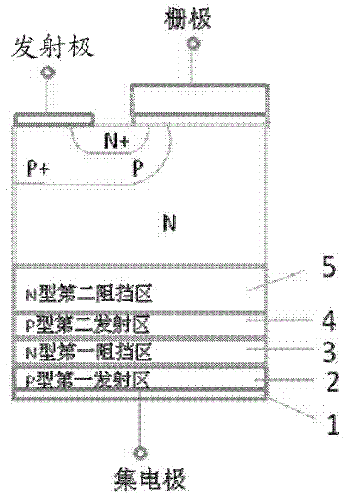
[0025] See image 3 As shown, it is the back structure of the novel insulated gate bipolar transistor of the present invention. The back of the silicon chip of the insulated gate bipolar transistor is sequentially connected with an N-type second barrier region 5, a P-type second emitter region 4, and an N-type first emitter region. Barrier region 3 and P-type first emitter region 2 and collector electrode 1, that is, the back structure is P / N / P / N + A structure combining multi-level emission regions and barrier regions, the thickness of the N-type second barrier region 5 is 0-10 μm, and the thickness can be controlled at 0.1 μm, 0.5 μm, 1 μm, 2 μm, 4 μm, 5 μm, 8 μm, 9 μm, 10 μm etc., preferably controlled between 0.1-5 μm, the injection efficiency of the above-mentioned two-stage emission region can be adjusted through the N-type second barrier region, and the electric field from the front can be blocked at the same time. The thickness of the P-type second emitter region 4 of ...


PUM


Abstract

The invention relates to a novel back structure of an insulated gate bipolar transistor, in which an N-type second barrier region, a P-type second emitter region, and an N-type first barrier region are sequentially connected from the inside to the outside of the silicon wafer of the insulated gate bipolar transistor. and a P-type first emitter region and a collector electrode, wherein the thickness of the N-type second barrier region is 0-10 μm, the thickness of the P-type second emitter region is 0.1-2 μm, and the thickness of the N-type first barrier region is 0.1-2 μm, and the thickness of the P-type first emitter region is 0.05-2 μm. The invention transforms the original back structure P-type level emission area into P / N / P / N + The structure combining the multi-level emitter region and the barrier region realizes the purpose of precisely controlling the hole distribution in the drift region, and solves the contradiction between ohmic contact and low injection efficiency while significantly improving the performance of the device. The coordination relationship between on-state characteristics and switching characteristics.

Description

technical field [0001] The invention relates to a novel back structure of an insulated gate bipolar transistor and a preparation method thereof, belonging to the technical field of semiconductor devices. Background technique [0002] Insulated gate bipolar transistor (IGBT) is a composite full-control voltage-driven power semiconductor device formed by combining bipolar transistors and insulated gate field effect transistors. It has the high input impedance of insulated gate field effect transistors and bipolar transistors. The advantages of low conduction voltage drop, simple driving circuit, and wide safe working area, no matter in the technical transformation of traditional industries, such as motor speed regulation, various high-frequency switching power supplies, etc., or in the development of new energy, such as Solar power generation, wind power generation and new energy vehicles, as well as emerging industries such as smart grids, rail transit, etc., as the core swit...

Claims


Application Information

Patent Timeline
Patent Type & Authority Patents(China)
IPC IPC(8): H01L29/06H01L29/739H01L21/331
CPCH01L29/0834H01L29/7395
Inventor 戚丽娜张景超刘利峰赵善麒林茂吴迪
Owner MACMIC SCIENCE & TECHNOLOGY CO LTD
Why Eureka
Try Eureka