Structural absorbing material

A wave absorbing material and structural technology, applied in the field of wave absorbing materials, can solve the problems of application limitation, deterioration of wave absorbing performance, etc., and achieve the effects of reduced sensitivity, widened wave absorbing incident angle, and small electrical size

Active Publication Date: 2011-12-21
XIDIAN UNIV
View PDF3 Cites 9 Cited by
  • Summary
  • Abstract
  • Description
  • Claims
  • Application Information

AI Technical Summary

Problems solved by technology

However, this structure can only absorb electromagnetic waves with a single polarization angle, and the absorption performance deteriorates rapidly with the increase of the incident angle of electromagnetic waves, and there is only a single absorption peak point, which constitutes a great limit to its application.

Method used


Image

  • Structural absorbing material
  • Structural absorbing material
  • Structural absorbing material

Examples


Embodiment 1

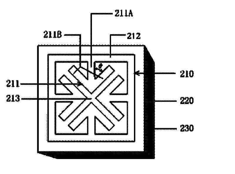
[0032] refer to figure 2 , the present invention selects double-sided copper-clad organic polymer dielectric substrate, and the substrate thickness is selected as λ / 68 according to the wavelength corresponding to the absorbing frequency band. One side of the substrate is etched with a metal pattern 210 , and the other side is not etched, which serves as an all-metal base plate 230 . The metal pattern 210 is composed of 4 metal wire arrows 211 pointing to the center and a regular quadrilateral metal wire frame 212. Two short lines 211B at the top of the 4 metal wire arrows 211 pointing to the center form a symmetrical cross structure. Glyph slit 213, the tail end of each metal wire arrow 211 is connected with regular quadrilateral metal wire frame 212, wherein the perimeter of regular quadrilateral metal wire frame 212 is 80λ / 100, two short lines 211B at the top of metal arrow 211, middle rod 211A and The line width of the metal wire frame 212 is λ / 120, the width of the cross...

Embodiment 2

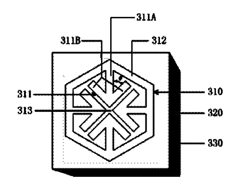
[0034] refer to image 3 , the present invention selects an inorganic ceramic dielectric substrate coated with copper on both sides, and the thickness of the substrate is selected as λ / 48 according to the wavelength corresponding to the absorbing frequency band. One side of the substrate is etched with a metal pattern 310 , and the other side is not etched, serving as a full metal base plate 330 . The metal pattern 310 is composed of 4 metal wire arrows 311 pointing to the center and a regular hexagonal metal wire frame 312. Two short lines 311B at the top of the 4 metal wire arrows 311 pointing to the center form a symmetrical cross structure. A cross-shaped gap 313, the tail end of each metal wire arrow 311 is connected to the regular hexagonal metal wire frame 312, wherein the perimeter of the regular hexagonal metal wire frame 312 is 82λ / 100, two short lines 311B at the top of the metal arrow 311, The line widths of the middle rod 311A ​​and the metal wire frame 312 are b...

Embodiment 3

[0036] refer to Figure 4 , the present invention selects double-sided copper-clad organic polymer dielectric substrates, and the thickness of the substrate is selected as λ / 55 according to the wavelength corresponding to the absorbing frequency band. One side of the substrate is etched with a metal pattern 410 , and the other side is not etched, which serves as a full metal base plate 430 . The metal pattern 410 is composed of 4 metal wire arrows 411 pointing to the center and a regular octagonal metal wire frame 412 with a perimeter of 88λ / 100, and the two short lines at the top of the 4 metal wire arrows 411 pointing to the center have a length of 56λ / 500 411B forms a symmetrical cross structure, in the middle of which there is a cross-shaped slit 413 with a width of λ / 140, and the angle between the two short lines 411B at the top of each metal wire arrow 411 and the rod 411A is θ=45°, and The tail end of each metal wire arrow 411 is connected to the regular octagonal meta...


PUM


Abstract

The invention discloses a structural wave-absorbing material, which mainly overcomes the defects of the prior art that only electromagnetic waves with a single polarization angle can be absorbed, the wave-absorbing entrance angle is narrow and only one wave-absorbing peak point exists. The structural wave-absorbing material is made of a medium substrate (220), the back face of the medium substrate (220) is a fully-metallic base plate (230), and the frontal face of the medium substrate (220) comprises an etched metallic pattern (210), wherein the metallic pattern (210) consists of four metallic line arrows (211) which point at the center and a regular polygonal metallic line frame (212) with sides having an even number which is more than 3 or a circular annular metallic line frame (512); two short lines (211B) at top ends of the four metallic line arrows form a symmetrical +-shaped cross structure, the middle of which is provided with a +-shaped gap (213) and the tail end of a middle bar (211A) of each metallic line arrow is connected with the metallic line frame. Compared with the prior art, the structural wave-absorbing material has the advantages of capability of absorbing electromagnetic waves with a random polarization angle, widening the wave-absorbing entrance angle and having two wave-absorbing peak points.

Description

technical field [0001] The invention belongs to the technical field of wave-absorbing materials, in particular to a structural wave-absorbing material, which can be used in conventional wave-absorbing applications and thermal imaging fields. technical background [0002] With the rapid development of electronic information technology, the role of wave-absorbing materials is becoming more and more important, and the requirements for them are getting higher and higher. Wave-absorbing materials are developing in the direction of stable performance, thin thickness, light weight, strong absorption, and simple preparation. . [0003] Common new absorbing materials mainly include the following types: ferrite, metal iron powder, polycrystalline iron fiber, acetylene carbon black, ceramic materials, and structural absorbing materials. Their advantages and disadvantages are as follows: [0004] Ferrite has the advantages of wide absorption frequency band and high absorption rate, bu...

Claims


Application Information

Patent Timeline
Patent Type & Authority Applications(China)
IPC IPC(8): H05K9/00
Inventor 李龙杨阳
Owner XIDIAN UNIV
Why Eureka
Try Eureka