

A loop multi-notch ultra-wideband antenna
An ultra-wideband antenna and loop technology, which is applied in loop antennas, antennas, antenna grounding devices, etc., can solve problems such as inconvenient debugging and production, increased antenna volume, electromagnetic wave leakage, etc., to reduce design costs, reduce overall volume, and widen impedance The effect of bandwidth
- Summary
- Abstract
- Description
- Claims
- Application Information
AI Technical Summary
Problems solved by technology
Method used
Image

Examples
Embodiment approach 1
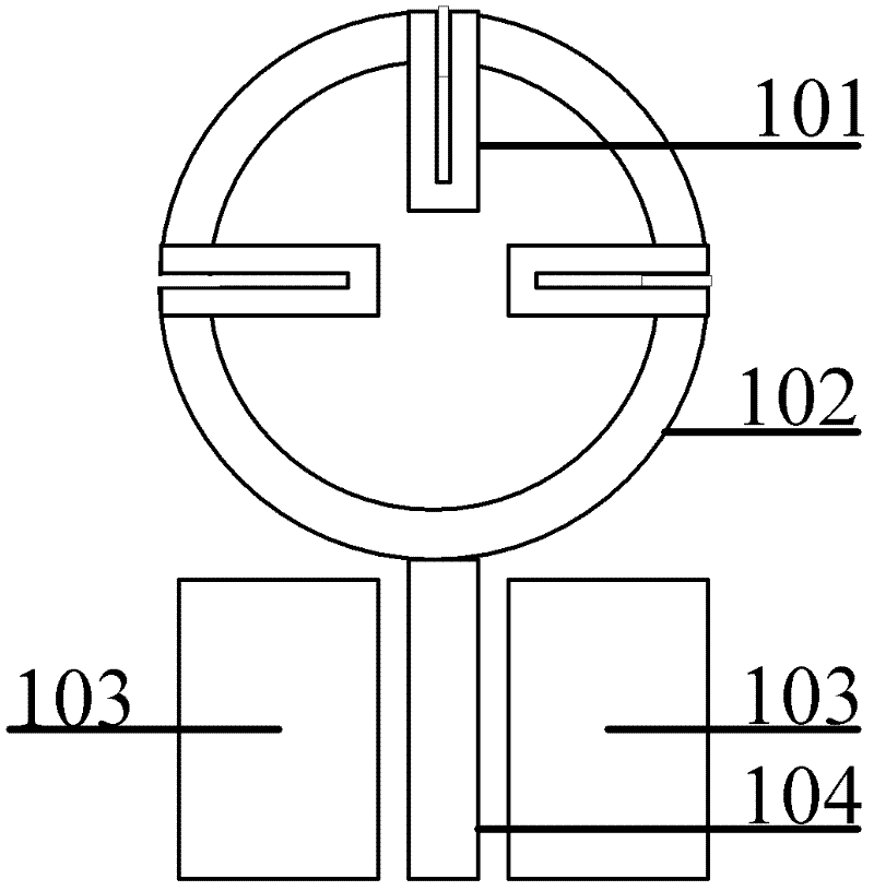
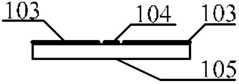
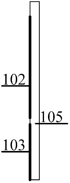
[0034] Such as figure 1 , figure 2 and image 3 shown. It consists of a slotted tuned microstrip line 101 , a ring radiation unit 102 , a coplanar waveguide ground plane 103 , a coplanar waveguide feeding signal stripline 104 and a dielectric substrate 105 . The lower end of the coplanar waveguide feeding signal stripline 104 of the antenna is connected to the inner conductor of the SMA. The outer conductor of the SMA is connected to the coplanar waveguide ground plane 103 . according to figure 1 , figure 2 and image 3 The structure shown, as long as the appropriate size is selected, can meet its ultra-wideband operating characteristics and multi-notch characteristics.
[0035] Design of antenna parameters:
[0036] 1. Selection of dielectric substrate
[0037] The dielectric constant of the dielectric substrate is generally between 2 and 9.8. The polytetrafluoroethylene board with a dielectric constant of 2.65 is used in the present invention. The price of the sub...
Embodiment approach 2
[0046] Such as Figure 4 As shown, two arc-shaped corners are cut off near the annular radiating element on the coplanar waveguide ground plane, which can not only improve the coupling capacitance and coupling inductance between the annular radiating element and the coplanar waveguide ground plane, but also increase the antenna's Impedance bandwidth. The antenna is composed of a tuned microstrip line 201, a ring radiation unit 202, a coplanar waveguide ground plane 203, a coplanar waveguide feeding signal stripline 204 and a dielectric substrate. The lower end of the coplanar waveguide feeding signal stripline 204 of the antenna is connected to the inner conductor of the SMA. The outer conductor of the SMA is connected to the coplanar waveguide ground plane 203 . In order to realize the notch characteristic, the slotted tuned microstrip line inside the annular radiating unit can be replaced by a tuned microstrip line, which can still meet the requirements of ultra-wideband c...
Embodiment approach 3
[0048] Such as Figure 5 As shown, the slotted tuned microstrip line and the tuned microstrip line are removed, and the antenna can be used as an ultra-wideband antenna. The antenna is composed of a ring radiation unit 302, a coplanar waveguide ground plane 303, and a coplanar waveguide feed signal stripline 304. and a dielectric substrate. The lower end of the coplanar waveguide feeding signal stripline 304 of the antenna is connected to the inner conductor of the SMA. The outer conductor of the SMA is connected to the coplanar waveguide ground plane 303 . The structure is simple, easy to design and implement, and easy to integrate with microwave integrated circuits.
PUM
| Property | Measurement | Unit |
|---|---|---|
| Thickness | aaaaa | aaaaa |
| Impedance | aaaaa | aaaaa |
Abstract
Description
Claims
Application Information