Passivation Method of Cavity Surface of f-p Cavity Semiconductor Laser

A laser and semiconductor technology, applied in the structure of optical resonant cavity, ion implantation plating, coating, etc., can solve the problem of inapplicability of GaN-based and ZnO-based semiconductor lasers, the inability to effectively reduce dangling bonds and surface states, and unfavorable Reduce laser cavity surface absorption and other problems, achieve the effect of increasing optical catastrophe damage threshold, improving stability and reliability, and increasing output power

Inactive Publication Date: 2011-12-28
苏州纳睿光电有限公司
View PDF3 Cites 15 Cited by
  • Summary
  • Abstract
  • Description
  • Claims
  • Application Information

AI Technical Summary

Problems solved by technology

Ordinary oxide coatings cannot effectively reduce the dangling bonds and surface states on the cavity surface of the F-P cavity semiconductor laser due to cleavage, which is not conducive to reducing the cavity surface absorption of the laser, and it is easy to cause the cavity surface of the laser to be recombined due to non-radiative recombination. Damaged by a sharp rise in temperature
For this reason, a layer of ZnSe or ZnS wide bandgap semiconductor material is epitaxially grown on the cavity surface as a passivation layer to reduce the dangling bonds of the laser cavity surface and the resulting light absorption, but due to the width of ZnSe or ZnS wide bandgap semiconductor material The bandgap width close to GaN, ZnO, etc. is only suitable for GaAs-based semiconductor lasers, but not for GaN-based and ZnO-based semiconductor lasers

Method used


Image

  • Passivation Method of Cavity Surface of f-p Cavity Semiconductor Laser
  • Passivation Method of Cavity Surface of f-p Cavity Semiconductor Laser
  • Passivation Method of Cavity Surface of f-p Cavity Semiconductor Laser

Examples


Embodiment 1

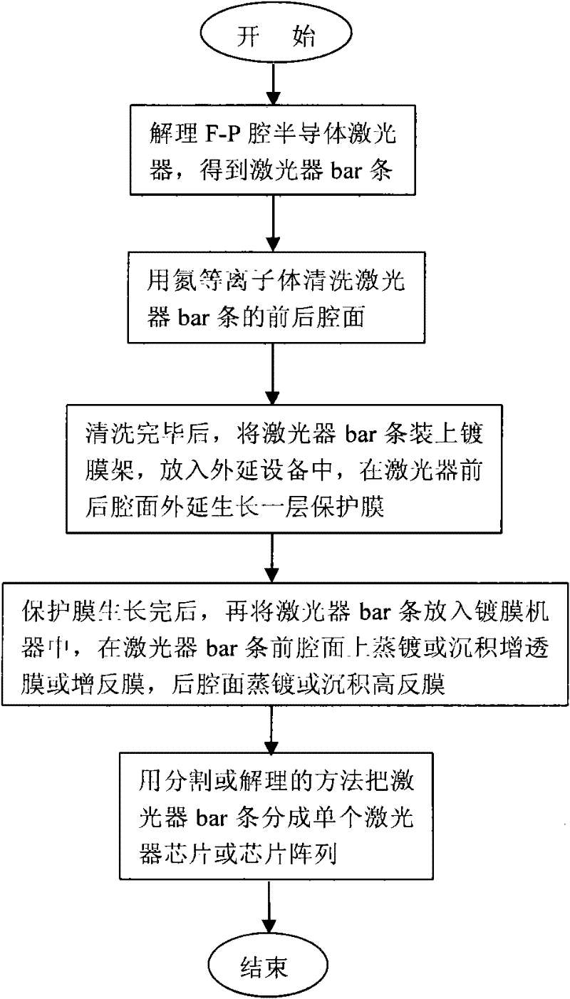
[0027] This embodiment uses a ridge-type GaN-based laser. The schematic diagram of the ridge GaN-based laser chip is attached figure 2 As shown, the active region of the laser is an InGaN / GaN multiple quantum well, and the top of the chip is a ridge type 1.

[0028] This method mainly comprises the following steps:

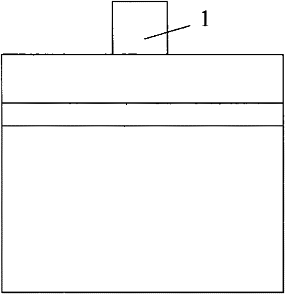
[0029] 1. Cleavage the F-P cavity-ridge GaN-based semiconductor laser to obtain a laser bar. The schematic diagram of the laser bar is attached image 3 shown;

[0030] 2. Clean the front and rear cavity surfaces of the laser bar with nitrogen plasma;

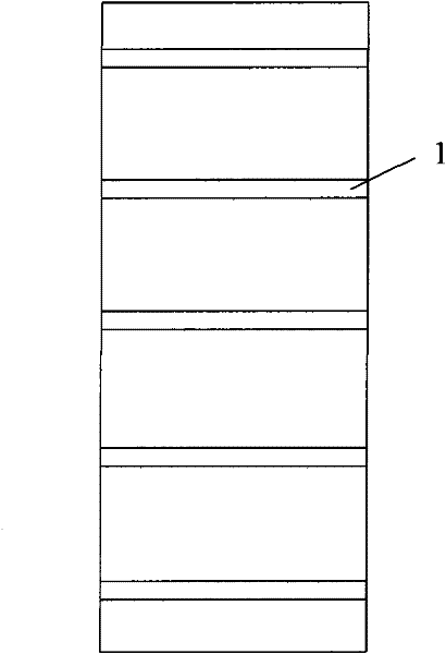
[0031] 3. After cleaning, install the laser bar on the coating frame, put it into the magnetron plasma sputtering system, and epitaxially grow a layer of AlON protective film 2 on the front and rear cavity surfaces of the laser, as attached Figure 4 shown. When epitaxially growing the AlON protective film 2, control its growth rate to be 2nm / min, not too fast, so that the epitaxial AlON protective film 2 gro...

Embodiment 2

[0036] This embodiment uses a ridge-type GaN-based laser. The schematic diagram of the ridge GaN-based laser chip is attached figure 2 As shown, the active region of the laser is an InGaN / GaN multiple quantum well, and the top of the chip is a ridge type 1.

[0037] This method mainly comprises the following steps:

[0038] 1. Cleavage the F-P cavity-ridge GaN-based semiconductor laser to obtain a laser bar. The schematic diagram of the laser bar is attached image 3 shown;

[0039] 2. Clean the front and rear cavity surfaces of the laser bar with nitrogen plasma;

[0040] 3. After cleaning, install the laser bar on the coating frame, put it into the electron cyclotron resonance plasma sputtering system, and epitaxially grow a layer of Al on the front and rear cavity surfaces of the laser 2 o 3 Protective film 2, if attached Figure 4 shown. Epitaxially grown Al 2 o 3 For protective film 2, control its growth rate to be 4nm / min, not too fast, so that the epitaxial Al...

Embodiment 3

[0045] This embodiment uses a ridge-type GaN-based laser. The schematic diagram of the ridge GaN-based laser chip is attached figure 2 As shown, the active region of the laser is an InGaN / GaN multiple quantum well, and the top of the chip is a ridge type 1.

[0046] This method mainly comprises the following steps:

[0047] 1. Cleavage the F-P cavity-ridge GaN-based semiconductor laser to obtain a laser bar. The schematic diagram of the laser bar is attached image 3 shown;

[0048] 2. Clean the front and rear cavity surfaces of the laser bar with nitrogen plasma;

[0049] 3. After cleaning, install the laser bar on the coating frame, put it into the MOCVD epitaxy equipment, and epitaxially grow a layer of SiAlON protective film 2 on the front and rear cavity surfaces of the laser, as attached Figure 4 shown. When epitaxially growing the SiAlON protective film 2, control its growth rate to be 5nm / min, not too fast, so that the epitaxial SiAlON protective film 2 grows on...


PUM


Abstract

A method for passivating the cavity surface of an F-P cavity semiconductor laser, comprising the following steps: 1, cleaving the F-P cavity semiconductor laser to obtain a laser bar; 2, cleaning the front and rear cavity surfaces of the laser bar with nitrogen plasma; 3, applying epitaxy Growth technology epitaxially grows a layer of protective film on the front and rear cavity surfaces of the laser; 4. Evaporate or deposit an anti-reflection film on the front cavity surface of the laser bar, and evaporate or deposit a high-reflection film on the rear cavity surface; 5. Use segmentation or solution A reasonable approach divides the laser bar into individual laser chips or chip arrays. The invention can effectively reduce the dangling bonds and surface states at the laser cavity surface, and suppress the light absorption of the laser cavity surface; at the same time, the epitaxially grown thin film is a wide bandgap material, which absorbs very little outgoing light, and can greatly suppress the laser cavity The light absorption at the surface and the resulting temperature rise improve the stability and reliability of the laser.

Description

technical field [0001] The invention relates to a cavity surface passivation method of an F-P cavity semiconductor laser, which is suitable for GaAs-based, InP-based, GaN-based and ZnO-based F-P cavity semiconductor lasers. Background technique [0002] Due to the advantages of small size, light weight and wide wavelength range, semiconductor lasers have been widely used in industry, military, medical and other fields. Stability and reliability are the prerequisites for using lasers. [0003] At the cavity surface of the semiconductor laser, the optical power density is high and the defect density is large. Defects such as dislocations will cause surface light absorption and non-radiative recombination. The heat generated by light absorption and non-radiative recombination will increase the temperature and cause a band gap. The local thermal contraction of , while the light absorption and non-radiative recombination will intensify with the increase of temperature, forming a ...

Claims


Application Information

Patent Timeline
Patent Type & Authority Applications(China)
IPC IPC(8): H01S5/10C23C14/35
Inventor 冯美鑫张书明王辉刘建平曾畅李增成王怀兵杨辉
Owner 苏州纳睿光电有限公司
Why Eureka
Try Eureka