Flash memory unit for shared source line and forming method thereof

A technology of flash memory cells and source lines, applied in electrical components, electric solid state devices, circuits, etc., can solve the problems of low programming efficiency of flash memory cells, achieve the effects of improving stress reliability, increasing coupling coefficient, and reducing thickness

Active Publication Date: 2012-01-11
SHANGHAI HUAHONG GRACE SEMICON MFG CORP
View PDF3 Cites 27 Cited by
  • Summary
  • Abstract
  • Description
  • Claims
  • Application Information

AI Technical Summary

Problems solved by technology

[0005] The problem to be solved by the present invention is to provide a flash memory unit sharing a source line and its forming method, so as to solve the problem that the programming efficiency of the flash memory unit sharing a source line in the existing structure is relatively low when the size of the device is reduced

Method used


Image

  • Flash memory unit for shared source line and forming method thereof
  • Flash memory unit for shared source line and forming method thereof
  • Flash memory unit for shared source line and forming method thereof

Examples


Embodiment Construction

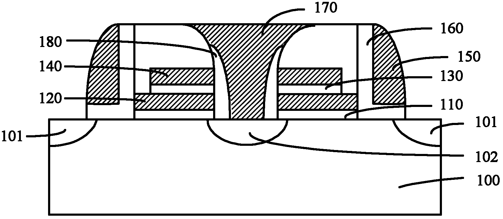
[0038] It can be known from the background art that when the device is scaled down, the performance of the existing flash memory unit sharing the source line is not good enough, and the programming efficiency is relatively low.

[0039] Please refer to figure 1 When programming the existing flash memory cells sharing the source line, the voltage applied to the source line 170 is coupled to the floating gate 120 through the spacer dielectric layer 180, and hot electrons migrate from the drain 101 to the source 102 under the action of the coupling voltage , and is injected into the floating gate 120 during the migration process. In order to ensure the data retention capability of the floating gate 120, the sidewall dielectric layer 180 must have no defects. Due to the limitation of the deposition process, if the thickness of the sidewall dielectric layer 180 is too small, some defects are prone to occur, such as defects such as voids formed in the film. Therefore, the thickness...


PUM


Abstract

The embodiment of the invention provides a flash memory unit for a shared source line and a forming method thereof. The provided flash memory unit for the shared source line comprises a semiconductor substrate, a source line, a floating gate dielectric layer, a floating gate, a control gate dielectric layer, a control gate, side wall dielectric layers, side walls, a tunneling oxide layer, a word line, a drain electrode and a source electrode, wherein the source line is positioned on the surface of the semiconductor substrate; the floating gate dielectric layer, the floating gate, the control gate dielectric layer and the control gate are sequentially positioned on the surface of the semiconductor substrate on two sides of the source line; the side wall dielectric layers are positioned between the source line and the floating gate as well we between the source line and the control gate; the side walls are positioned on the floating gate and the control gate, which are far from the source line; the tunneling oxide layer is adjacent to the side wall and is positioned on the surface of the semiconductor substrate; the word line is positioned on the surface of the tunneling oxide layer; the drain electrode is positioned in the semiconductor substrate at one side of the word line, which is far from the source line; the source electrode is positioned in the semiconductor substrate which is right opposite to the source line; and the floating gate is provided with a p-type doping end which is close to the source line, wherein the doping type of the floating gate is in a p type and the doping type of other parts is respectively in an n type.

Description

technical field [0001] The invention relates to a semiconductor device and its forming method, in particular to a flash memory unit sharing a source line and its forming method. Background technique [0002] In the current semiconductor industry, integrated circuit products can be mainly divided into three types: analog circuits, digital circuits and digital / analog hybrid circuits, among which storage devices are an important type of digital circuits. In recent years, among storage devices, a flash memory (flash memory, referred to as a flash memory unit) has developed particularly rapidly. The main feature of the flash memory unit is that it can keep the stored information for a long time without power on; and it has the advantages of high integration, fast access speed, easy erasing and rewriting, etc. Has been widely used. [0003] figure 1 It is a schematic structural diagram of an existing flash memory unit sharing a source line, including: a semiconductor substrate ...

Claims


Application Information

Patent Timeline
Patent Type & Authority Applications(China)
IPC IPC(8): H01L29/40H01L27/115H01L21/8247
Inventor 曹子贵
Owner SHANGHAI HUAHONG GRACE SEMICON MFG CORP
Why Eureka
Try Eureka