Manufacturing method of phase change memory storage unit

A technology of phase-change memory and storage unit, which is applied in the direction of electrical components, semiconductor devices, electric solid-state devices, etc., and can solve the problems of reducing the yield rate of phase-change memory, increasing the poor contact between the bottom electrode and the phase-change layer, and damage to the storage unit of the phase-change memory and other issues to achieve the effect of avoiding partial discharge phenomenon

Active Publication Date: 2013-10-30
SEMICON MFG INT (SHANGHAI) CORP +1
View PDF5 Cites 0 Cited by
  • Summary
  • Abstract
  • Description
  • Claims
  • Application Information

AI Technical Summary

Problems solved by technology

in use figure 1 In the process of forming the storage unit of the phase change memory according to the scheme, the step of pre-cleaning the contact surface of the bottom electrode 101 by plasma bombardment is included. During the pre-cleaning process, the surface of the patterned low dielectric constant material layer 104 will be damaged Partial discharge phenomenon, which will lead to damage or even failure of the final phase change memory storage unit produced
In order to prevent the above problems, two methods can be adopted: the first method skips the pre-cleaning step and directly deposits the phase change layer, but due to the small contact area between the bottom electrode and the phase change layer, plus the deposited phase Each process step before the phase change layer is obtained by the change material will contaminate the contact surface of the bottom electrode, thereby greatly increasing the probability of poor contact between the bottom electrode and the phase change layer, and greatly reducing the quality of the final phase change memory. The second method, in the pre-cleaning process, reduces the RF power and time of plasma bombardment, thereby reducing the occurrence of partial discharge on the surface of the low dielectric constant material layer, but this does not completely avoid the occurrence of partial discharge

Method used


Image

  • Manufacturing method of phase change memory storage unit
  • Manufacturing method of phase change memory storage unit
  • Manufacturing method of phase change memory storage unit

Examples


Embodiment Construction

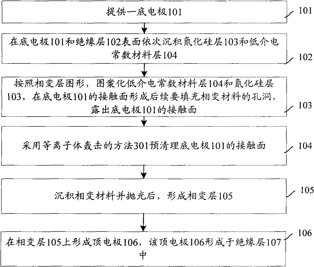
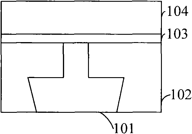
[0037] In order to make the object, technical solution and advantages of the present invention clearer, the present invention will be further described in detail below with reference to the accompanying drawings and examples.

[0038] In the present invention, in order to avoid the partial discharge phenomenon in the pre-cleaning process when making the phase change memory storage unit, and to prevent the final phase change memory storage unit from being damaged, the gas phase deposition method is used to be affected by the holes to form the phase change layer. Obviously, while the method of plasma bombardment is affected by the small characteristics of the holes to form the phase change layer, the following method is adopted:

[0039] Before the contact surface of the bottom electrode 101 is pre-cleaned by plasma bombardment, a layer of phase change material is deposited as a sacrificial layer and a protective layer for cleaning the bottom electrode 101 . Because the aspect r...


PUM

PropertyMeasurementUnit
thicknessaaaaaaaaaa

Abstract

The invention discloses a manufacturing method of a phase change memory storage unit. The method comprises the following steps of: forming a bottom electrode in a first insulation layer and then sequentially depositing a silicon nitride layer and a low-dielectric-constant material layer; patterning the low-dielectric-constant material layer and the silicon nitride layer to form a hole, exposing the contact surface of the bottom electrode out of the hole, and depositing a first phase change material in the hole; precleaning the first phase change material by adopting a plasma bombarding method till the contact surface of the bottom electrode is exposed, and depositing a second phase change material to fill the hole; polishing the deposited second phase change material to the surface of the hole to form a phase change layer; and forming a top electrode on the phase change layer and forming the top electrode in the second insulation layer. According to the invention provided by the invention, the local discharge phenomenon occurring in the precleaning process is avoided, and the finally manufactured phase change memory storage unit cannot be damaged.

Description

technical field [0001] The invention relates to the technical field of semiconductors, in particular to a method for manufacturing a storage unit of a phase-change memory. Background technique [0002] At present, Phase-Change RAM (PC RAM) has non-volatility, long cycle life, small component size, low power consumption, multi-level storage, high-efficiency reading, radiation resistance, high and low temperature resistance, The advantages of anti-vibration, anti-electronic interference and simple manufacturing process are considered to be the most likely to replace the current flash memory (Flash), dynamic random access memory (DRAM) and static memory (SRAM) and become the mainstream product of semiconductor memory in the future. [0003] A PC RAM memory cell includes a phase change layer, and bottom and top electrodes in contact with the phase change layer. The phase change layer of the PC RAM storage unit is the core area of ​​the phase change memory, which is used for the...

Claims


Application Information

Patent Timeline
Patent Type & Authority Patents(China)
IPC IPC(8): H01L45/00H01L27/24
Inventor 周真向阳辉冯永刚任万春
Owner SEMICON MFG INT (SHANGHAI) CORP
Why Eureka
Try Eureka