Near-infrared quantum cutting transparent film and preparation method thereof
A quantum tailoring, transparent film technology, applied in chemical instruments and methods, ion implantation plating, coating and other directions, can solve the problems of serious powder scattering, limit the practical application of solar cells, poor transparency, etc., to improve the conversion efficiency, Improve the effect of low work efficiency and improve utilization efficiency
- Summary
- Abstract
- Description
- Claims
- Application Information
AI Technical Summary
Problems solved by technology
Method used
Image
Examples
Embodiment 1
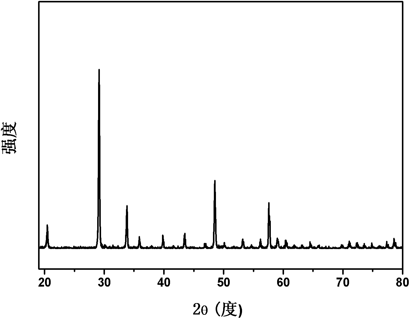
[0022] (1) in Y 2 o 3 Add Bi to the powder 2 o 3 Powder and Yb 2 o 3 powder, where Bi 2 o 3 Powder mole fraction is 0.25%, Yb 2 o 3 The molar fraction of the powder is 2.5%, and then mixed by ball milling, dried and calcined at 1200°C for 12 hours, and the powder is pressed into a ceramic target by hot pressing. The XRD pattern of its ceramic target material (see figure 1 ) exactly matches Y 2 o 3 PDF 41-1105 Diffraction Standard Spectrum.
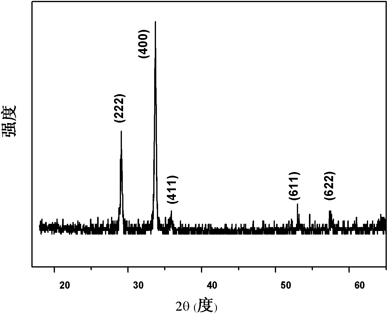
[0023] (2) Y made by step (1) 2 o 3 :Bi, Yb ceramic target, using laser pulse deposition method, using silicon wafer as substrate, passing O with a purity of 99.999% 2 , the substrate temperature is 500°C, the target-base distance is 6cm, the working pressure is 1Pa, the laser energy is 350mJ / pulse, and the deposition time is 90min. get pure phase Y 2 o 3 film, its XRD pattern is shown in figure 2 . Use FLS920 fluorescence spectrometer to measure the emission spectrum at room temperature under the excitation condition o...
Embodiment 2
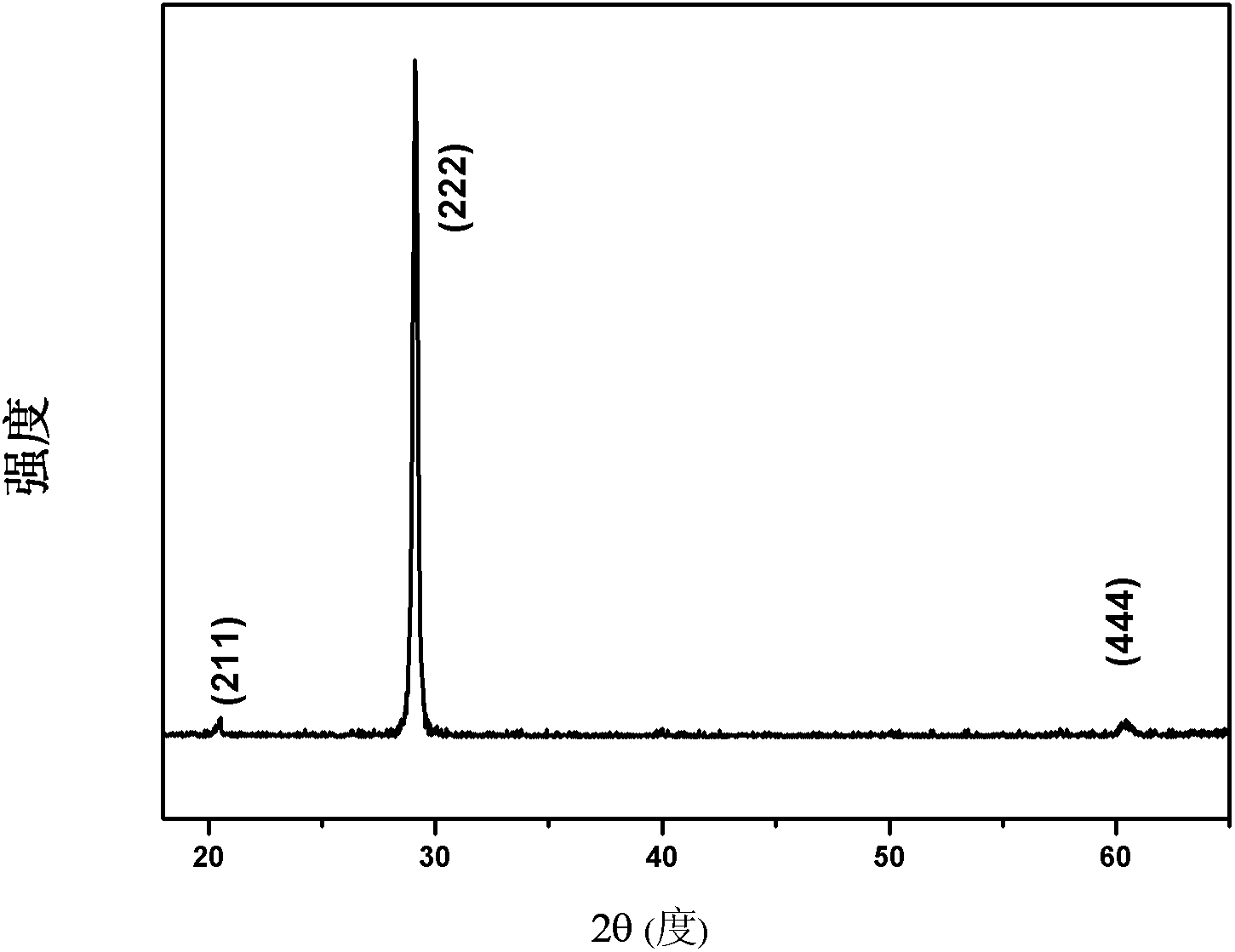
[0025] Substrate temperature is 700 ℃, and other preparation conditions are the same as embodiment 1, and the XRD pattern of obtained thin film is shown in image 3 . Use FLS920 fluorescence spectrometer to measure the emission spectrum at room temperature under the excitation condition of 331nm, it is observed that the corresponding Yb 3+ : 2 f 5 / 2 → 2 f 7 / 2 Transition quantum tailoring near-infrared light emission band (central wavelength 976nm). Its quantum efficiency has been measured to exceed 152%.
Embodiment 3
[0027] (1) in Y 2 o 3 Add Bi to the powder 2 o 3 Powder and Yb 2 o 3 powder, where Bi 2 o 3 Powder mole fraction is 0.25%, Yb 2 o 3 The molar fraction of the powder is 2.5%, and then mixed by ball milling, dried and calcined at 1200°C for 12 hours, and the powder is pressed into a ceramic target by hot pressing. The XRD pattern of its ceramic target material (see figure 1 ) exactly matches Y 2 o 3 PDF 41-1105 Diffraction Standard Spectrum.
[0028](2) Y made by step (1) 2 o 3 :Bi, Yb ceramic target material, using the laser pulse deposition method, using the quartz plate as the substrate, passing O with a purity of 99.999% 2 , the substrate temperature is 700°C, the target-base distance is 6cm, the working pressure is 1Pa, the laser energy is 350mJ / pulse, and the deposition time is 90min. Obtain a pure phase transparent Y 2 o 3 Thin films, the average transmittance of which exceeds 90% at 400-800nm, such as Image 6 shown. Use FLS920 fluorescence spectromete...
PUM
| Property | Measurement | Unit |
|---|---|---|
| quantum efficiency | aaaaa | aaaaa |
| quantum efficiency | aaaaa | aaaaa |
| quantum efficiency | aaaaa | aaaaa |
Abstract
Description
Claims
Application Information


