

Method for rapidly preparing large-area and uniform black silicon material, and device thereof
A large-area, black silicon technology, applied in chemical instruments and methods, crystal growth, electrical components, etc., can solve the problems of poor surface microstructure uniformity, low efficiency, and inability to meet mass production, and achieve high preparation efficiency and uniformity Good results
- Summary
- Abstract
- Description
- Claims
- Application Information
AI Technical Summary
Problems solved by technology
Method used
Image

Examples
Embodiment Construction
[0028] In order to describe the technical content, structural features, achieved goals and effects of the present invention in detail, the following will be described in detail in conjunction with specific embodiments and accompanying drawings.
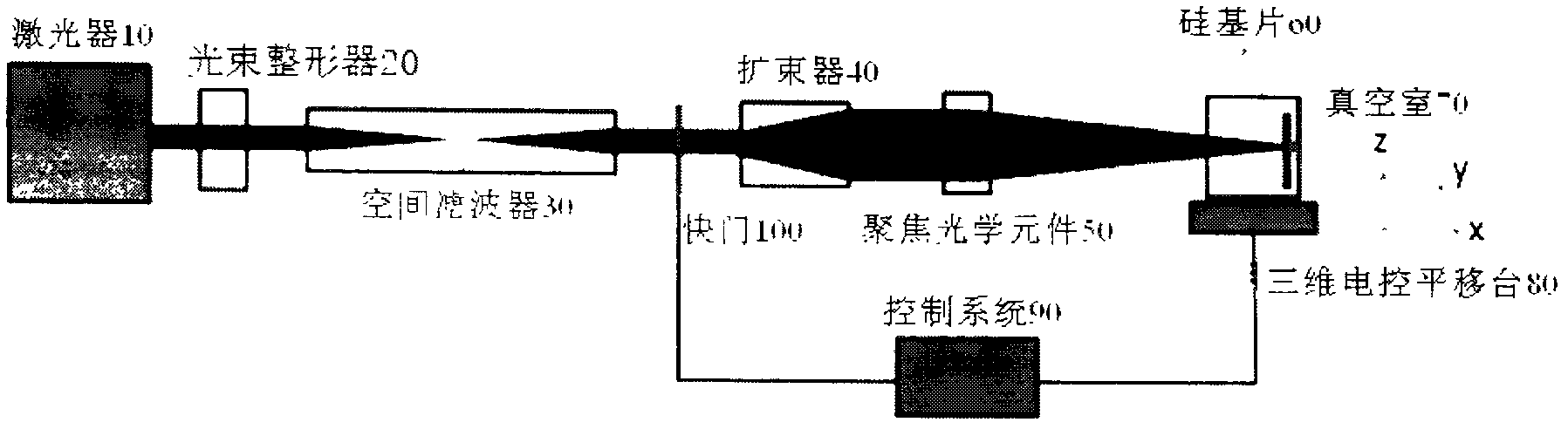
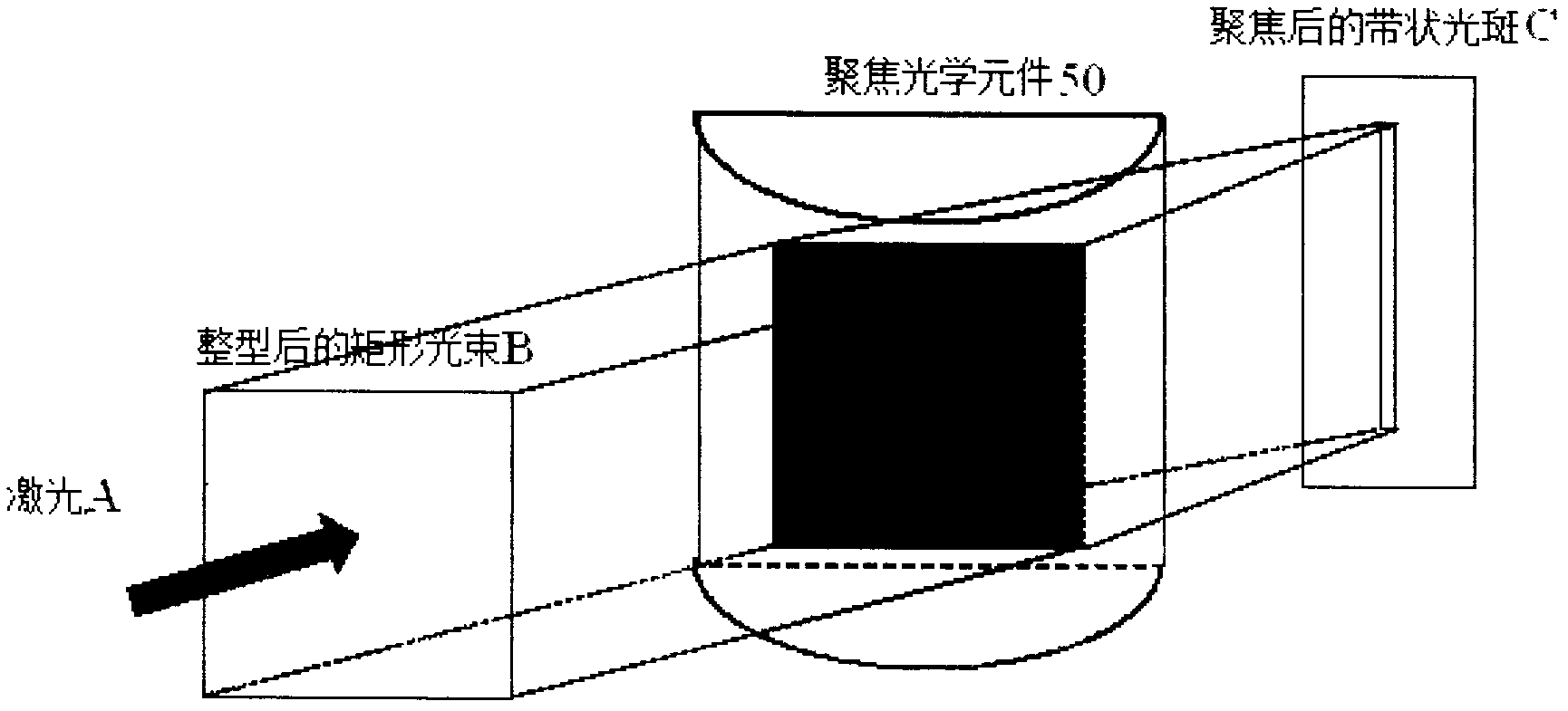
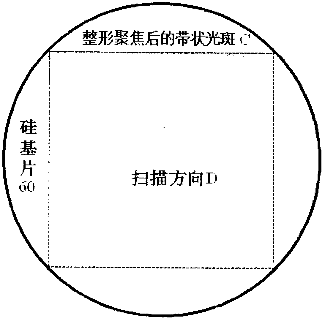
[0029] The invention discloses a method and equipment for rapidly preparing large-area black silicon materials by using pulsed laser raster scanning. figure 1It is a schematic diagram of the equipment structure and laser light path for rapid preparation of black silicon materials. The laser 10 emits a pulsed laser beam with a pulse width ranging from femtoseconds to milliseconds, including femtoseconds, picoseconds, nanoseconds, etc.; the output frequency of the laser 10 ranges from 0.1-100K Hz, and the single pulse energy output by the laser 10 ranges from Joule - 1000 Joule range. Because the beam output by the laser 10 is generally a circular beam, in order to obtain a surface microstructure with uniform physical and chemical prop...
PUM
 Abstract
Description
Claims
Application Information