Metal film resistor structure and manufacturing method thereof

一种金属薄膜电阻、制造方法的技术,应用在电阻器、半导体/固态器件制造、电路等方向,能够解决金属薄膜电阻易于损伤等问题,达到提高可靠性的效果

Active Publication Date: 2012-01-18
SHANGHAI INTEGRATED CIRCUIT RES & DEV CENT
View PDF7 Cites 8 Cited by
  • Summary
  • Abstract
  • Description
  • Claims
  • Application Information

AI Technical Summary

Problems solved by technology

[0007] The purpose of the present invention is to provide a metal thin film resistor structure and its manufacturing method to solve the problem that the metal thin film resistor is easy to be damaged in the existing process of adding a photolithography mask to form a metal thin film resistor structure

Method used


Image

  • Metal film resistor structure and manufacturing method thereof
  • Metal film resistor structure and manufacturing method thereof
  • Metal film resistor structure and manufacturing method thereof

Examples


Embodiment 1

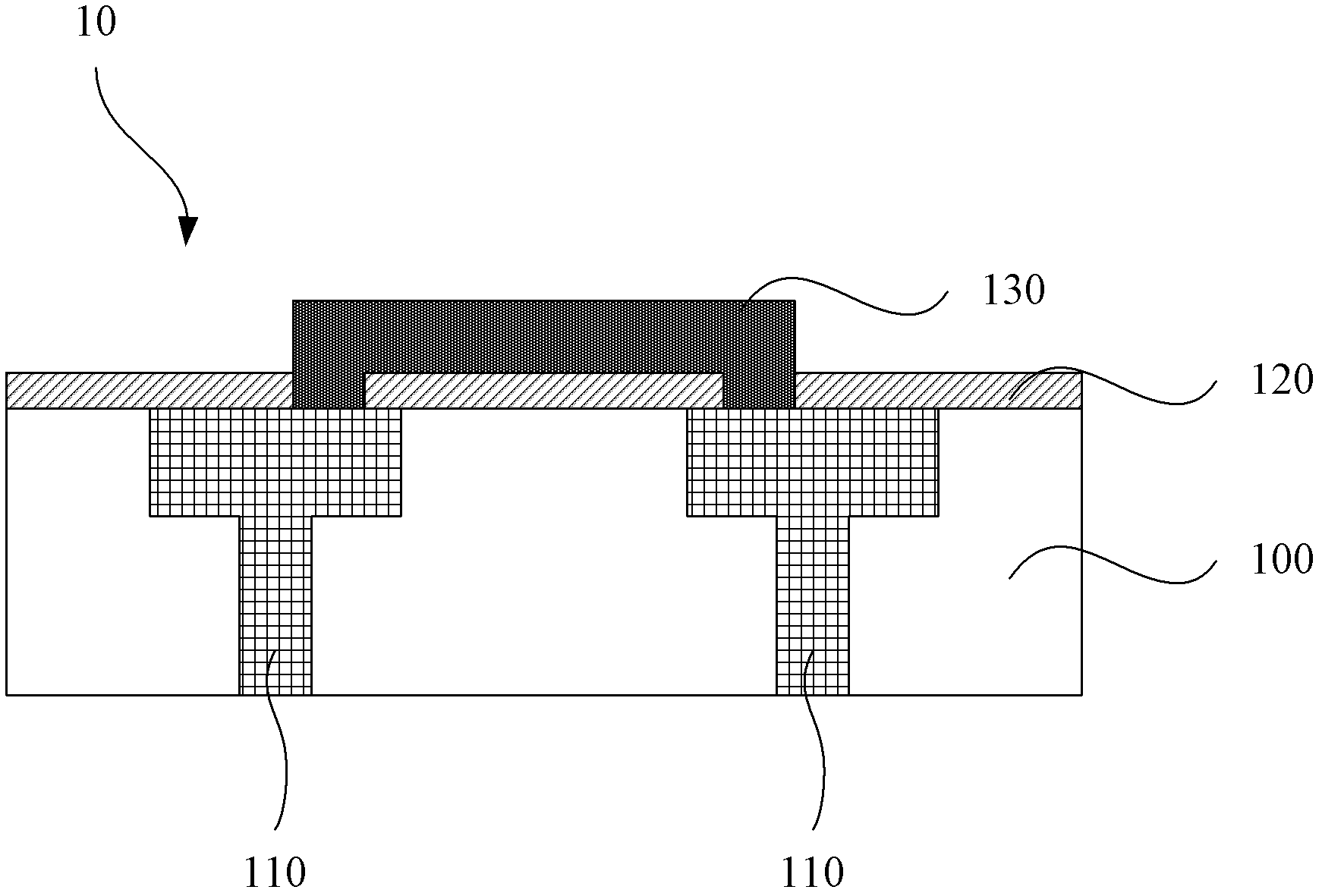
[0052] Please refer to Figure 3a ~ 3f , which is a schematic cross-sectional view of the manufacturing method of the metal thin film resistor structure according to Embodiment 1 of the present invention.

[0053] Such as Figure 3a As shown, firstly, an insulating layer 300 is provided, and an underlying metal copper interconnection line 310 is formed in the insulating layer 300 . The material of the insulating layer 300 can be SiO 2 , FSG (fluorine-doped silicon dioxide, SiOF) and other low-K dielectric materials.

[0054] Such as Figure 3b As shown, secondly, a capping layer 320 is formed on the insulating layer 300 and the underlying metal copper interconnection 310 . In this embodiment, the capping layer 320 includes: a diffusion barrier layer 321 and a thickened layer 322 . The diffusion barrier layer 321 can prevent the copper diffusion in the lower metal copper interconnection line 310 , the material of which can be silicon nitride or silicon carbide, and the thi...

Embodiment 2

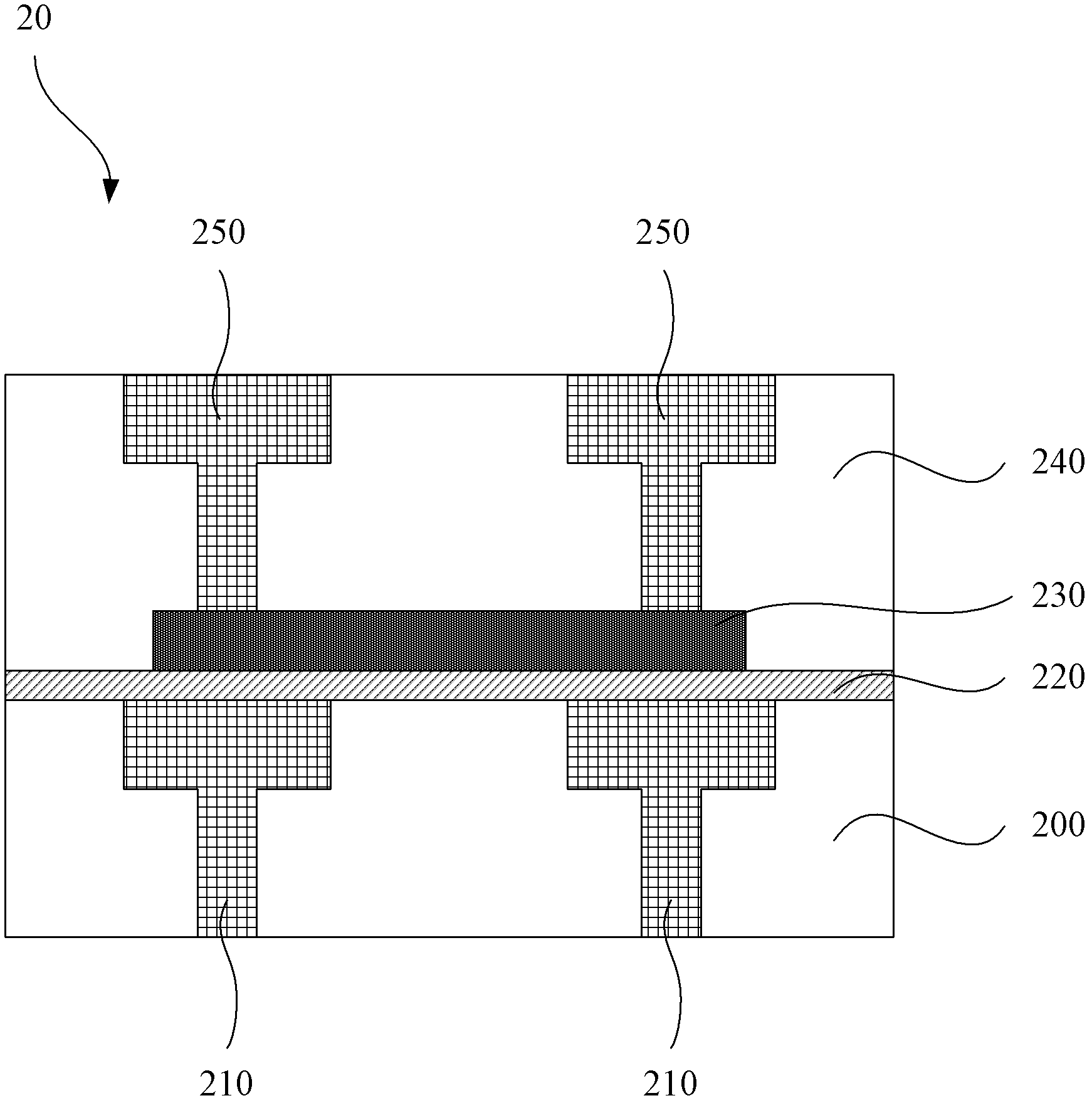
[0062] Please refer to Figure 5a-5f , which is a schematic cross-sectional view of the manufacturing method of the metal thin film resistor structure according to the second embodiment of the present invention.

[0063] Such as Figure 5a As shown, firstly, an insulating layer 500 is provided, and an underlying metal copper interconnection line 510 is formed in the insulating layer 500 . The material of the insulating layer 500 can be SiO 2 , FSG and other low K dielectric materials.

[0064] Such as Figure 5b As shown, secondly, a capping layer 520 is formed on the insulating layer 500 and the underlying metal copper interconnection 510 . In this embodiment, the capping layer 520 is a diffusion barrier layer. The diffusion barrier layer can block the copper diffusion in the lower metal copper interconnection 510 , and its material can be silicon nitride or silicon carbide, and the thickness of the diffusion barrier layer can be 150 angstroms to 700 angstroms.

[0065]...

Embodiment 3

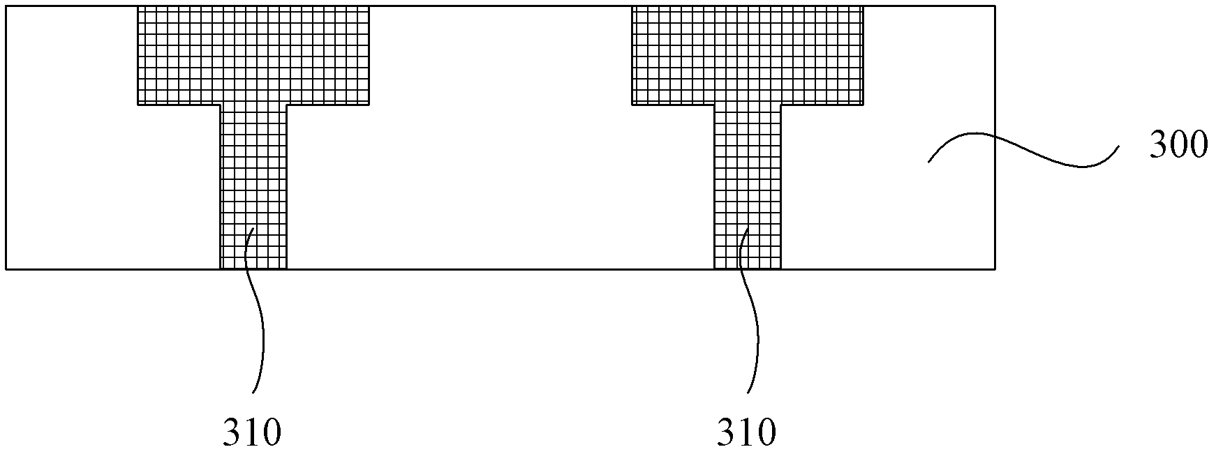
[0071] Please refer to Figure 6a~6c , which is a schematic cross-sectional view of the manufacturing method of the metal thin film resistor structure according to the third embodiment of the present invention.

[0072] Such as Figure 6a As shown, firstly, an insulating layer 600 is provided, and an underlying metal copper interconnection line 610 is formed in the insulating layer 600 . The material of the insulating layer 600 can be SiO 2 , FSG and other low K dielectric materials.

[0073] Such as Figure 6b As shown, next, a metal thin film layer 620 is formed on the insulating layer 600 and the underlying metal copper interconnection 610 . In this embodiment, the metal thin film layer 620 may be formed by a physical vapor deposition process, a chemical vapor deposition process or an atomic layer deposition process, and the thickness of the metal thin film layer 620 may be 50 angstroms to 2000 angstroms. The material of the metal thin film layer 620 can be W, WN x , ...


PUM


Abstract

The invention provides a metal film resistor structure and a manufacturing method thereof. The metal film resistor structure can be formed by adding a photoetching mask plate, wherein a metal film resistor is connected with a lower layer metallic copper interconnecting wire. The metal film resistor structure solves the problem of etch damage to the metal film resistor during the formation of an upper layer metallic copper interconnecting wire in the prior art, and then improves the reliability of the formed metal film resistor.

Description

technical field [0001] The invention relates to the technical field of integrated circuits, in particular to a metal thin film resistance structure and a manufacturing method thereof. Background technique [0002] Integrated circuits are developing along Moore's Law, and the requirements for device and system performance are getting higher and higher, and it is becoming more and more important to integrate passive devices and active devices on the same chip. With the development of SOC, RF and other circuits, the highly integrated, high-precision and high-reliability passive components—resistors have attracted the attention of many design companies and chip manufacturers. [0003] The resistors integrated on the chip generally include buried layer resistors, well resistors, polysilicon resistors and metal film resistors. Among them, the metal thin film resistor can be integrated in the back-end process without additionally increasing the chip area, thereby reducing the cost...

Claims


Application Information

Patent Timeline
Patent Type & Authority Applications(China)
IPC IPC(8): H01L27/00H01L21/02
CPCH01L28/24H01L23/5228H01L28/20H01L23/53238H01L2924/0002H01L2924/00
Inventor 左青云康晓旭曾少海
Owner SHANGHAI INTEGRATED CIRCUIT RES & DEV CENT
Why Eureka
Try Eureka