Four-tube active pixel of rapid charge transfer and making method thereof

A fast, pixel-based technology, applied in circuits, transistors, electrical components, etc., to solve problems such as limiting the application of CMOS image sensors, deteriorating pixel random noise, and image smearing

Active Publication Date: 2012-01-18
TIANJIN UNIV
View PDF3 Cites 14 Cited by
  • Summary
  • Abstract
  • Description
  • Claims
  • Application Information

AI Technical Summary

Problems solved by technology

The above-mentioned traditional PPD 4T-APS faces serious bottlenecks in this respect: on the one hand, due to the conversion of charges into voltages and the corresponding conversion node reset process, active pixels need to perform correlated double sampling of the FD reset voltage and the FD light-induced voltage , so that the fixed pattern noise and reset noise can be eliminated to output a low-noise readout signal equivalent to a CCD pixel
Compared with the simple charge transfer between CCD pixels, at the same frame readout rate, the time Ttf for PPD 4T-APS charge transfer is shorter than that of CCD pixels; on the other hand, since CMOS pixels are compatible with standard CMOS processes, The reset voltage of the TG gate and FD is much lower than that of the CCD pixel, the potential well depth difference ΔΦ from the PD to the FD is small, and the electric field pointing to the TX direction at the edge of the PD far away from the TX is weak, resulting in a sense of The speed of the generated charge Q moving towards TX slows down
Therefore, under the condition of the same PD size and frame readout rate, it is more difficult for PPD 4T-APS pixels to achieve rapid and complete transfer of induced charges than CCD pixels, and it is easier to leave residual charges in PDs.
This kind of charge residue will not only bring serious image smearing, but also further deteriorate the random noise of pixels, which ultimately limits the application of CMOS image sensors in high-end imaging fields.

Method used


Image

  • Four-tube active pixel of rapid charge transfer and making method thereof
  • Four-tube active pixel of rapid charge transfer and making method thereof
  • Four-tube active pixel of rapid charge transfer and making method thereof

Examples


Embodiment Construction

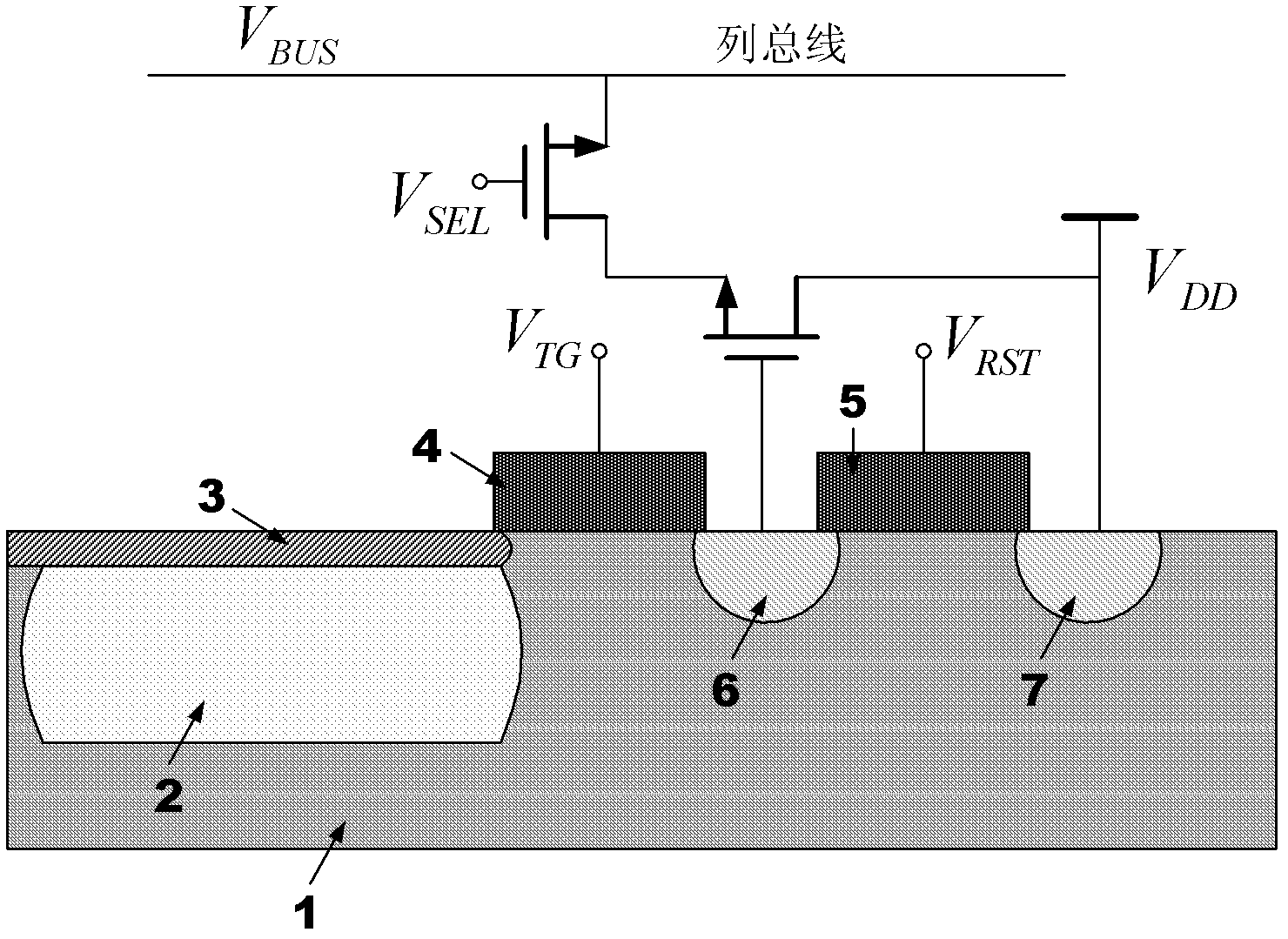
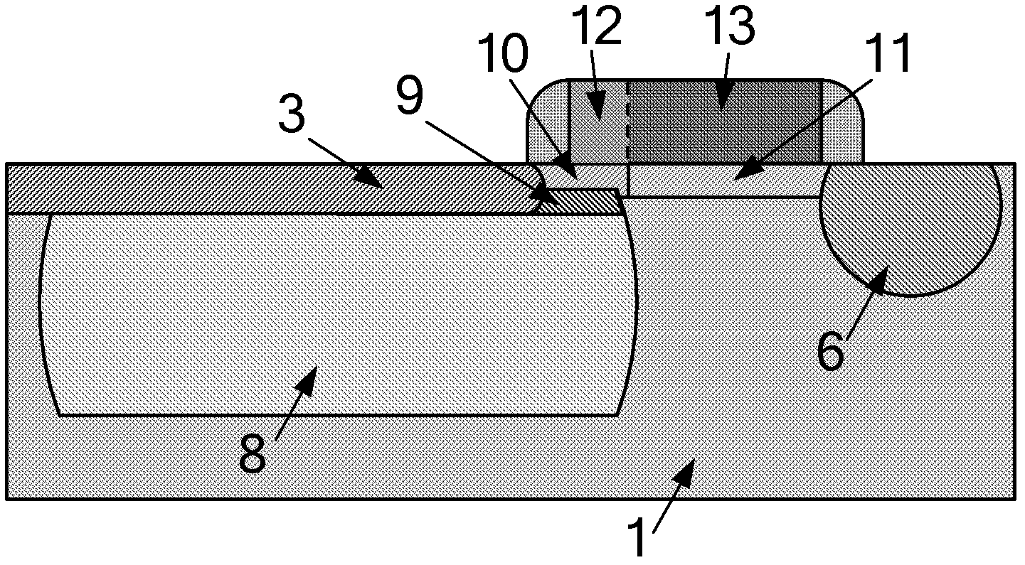
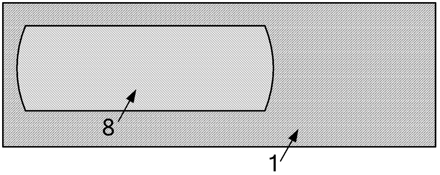
[0031] see figure 2 In the present invention, the N-type silicon semiconductor injection layers 8 and 9 of the photodiode are formed by implanting N-type impurities on the P-type silicon semiconductor substrate 1 . There is a certain overlap between the layout position of the N-type injection layer of the photodiode and the layout position of the polysilicon gate of the transmission tube, and the size of the overlapping area is generally between 5% and 50% of the gate length. The peak concentration of the N-type silicon semiconductor injection layer is close to the surface of the silicon semiconductor, and the N-type doping concentration in the overlapping region is the highest (position No. 9 in the figure), and its doping concentration ranges from 1e15 to 1e19 / cm 3 , and the concentration of the rest ranges from 1e14 to 1e18 / cm 3 Between, gradually decreasing from the overlapping region to the edge of the N-type implanted layer. A high concentration (1e18~1e20 / cm 3 ), the ...


PUM


Abstract

The invention belongs to the field of integrated circuit design and integrated circuit process of microelectronics and relates to a four-tube active pixel of rapid charge transfer. The four-tube active pixel of the rapid charge transfer comprises a photoelectric diode, a transmission tube, a reset tube, a source follower and a gate tube which are made on a P type substrate, wherein a region N of the photoelectric diode comprises a first N type injection layer and a second N type injection layer with lower dosage concentration, wherein the second N type injection layer is arranged on the firstN type injection layer; layout positions of the two N type injection layers and a polysilicon gate of the transmission tube exist an overlapped region; a P type silicon semiconductor injection layer with unbalanced dosage concentration is arranged in the overlapped region and an under-gate region of the transmission tube; the dosage concentration of the P type silicon semiconductor injection layer is highest in the overlapped region; the dosage of the grid of the polycrystalline silicon of the transmission tube is N- dosage on one side of the overlapped region and N+ dosage on one side of a non-overlapped region; and a clamping layer is arranged between the non-overlapped region of the region N of the photoelectric diode and the silicon surface. Meanwhile, the invention provides a making method of the active pixel. The pixel provided by the invention can obtain rapid charge transfer without tailing.

Description

technical field [0001] The invention relates to the field of integrated circuit design and integrated circuit technology of microelectronics, in particular to a four-transistor active pixel sensor (4transistors active pixel sensor, 4T APS) with fast charge transfer and a manufacturing method thereof. Background technique [0002] With the continuous reduction of the standard CMOS logic process and the continuous improvement of the CMOS image sensor (CMOS Image Sensors, CIS) manufacturing process, the CMOS image sensor continues to exert its advantages over the CCD image sensor in terms of integrability, power consumption, and random addressing. Relative advantages, becoming the mainstream device in the field of solid-state image sensors. Pinned-Photodiode Four Transistors-Active Pixel Sensor (PPD 4T-APS) based on clamping diodes has the characteristics of low dark current, can eliminate reset noise and low image smearing, and is currently the main pixel used in CIS structur...

Claims


Application Information

Patent Timeline
Patent Type & Authority Applications(China)
IPC IPC(8): H01L27/146H01L31/102H01L31/0352
CPCH01L27/14616H01L27/14689H01L27/146H01L31/102
Inventor 姚素英高志远徐江涛赵士彬李伟平
Owner TIANJIN UNIV
Why Eureka
Try Eureka