Precision current sensing element and manufacturing method thereof

A current sensing and precise technology, applied in resistor manufacturing, electrical components, resistor components, etc., can solve the problems of products unable to develop into miniaturization, reduce product performance, ceramic chip rupture, etc., to improve the current resistance capability, The effect of reducing product resistance and cost

Active Publication Date: 2013-03-27
NANJING SART SCI & TECH DEV
View PDF6 Cites 0 Cited by
  • Summary
  • Abstract
  • Description
  • Claims
  • Application Information

AI Technical Summary

Problems solved by technology

Reduced efficiency, reduced yield, and sharply increased costs
[0005] As described in the document CN201117381Y, the resistance layer is attached to the ceramic substrate by means of an adhesive layer. The only way to increase the power is to reduce the resistance by continuously superimposing single-layer products, and the superposition of alloy sheets is also accompanied by the increase of ceramic sheets. , in this way, the thickness of the product increases sharply, and the overlapping of different layers of ceramic sheets is also a big problem, and the lamination of multi-layer ceramics is more likely to cause the ceramic sheets to crack and reduce product performance
Affected by the thickness of the product, the product cannot be miniaturized. In today's increasingly miniaturized products, it is obviously an unsatisfactory process.

Method used


Image

  • Precision current sensing element and manufacturing method thereof
  • Precision current sensing element and manufacturing method thereof
  • Precision current sensing element and manufacturing method thereof

Examples


Embodiment 1

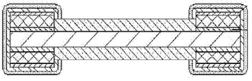
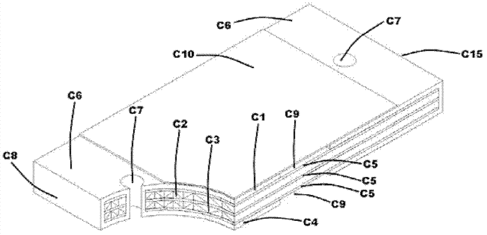
[0065] The inner layer is prepared by setting a sheet-shaped resistance alloy L6 on both sides of a piece of insulating heat-conducting adhesive, such as Figure 7 As shown, in this embodiment, L6 is closely combined with the insulating and thermally conductive adhesive C5 by pressing. The resistance alloy can be a material with a small temperature coefficient of resistance, and the resistivity is not limited; the insulating and heat-conducting adhesive can use a single high-molecular polymer glue with good heat resistance, insulation, thermal conductivity, and adhesion, or it can be passed through Glass fiber reinforced high molecular polymer glue with good heat resistance, insulation, thermal conductivity and adhesion. Then make the circuit on the inner layer after pressing, that is, the resistance alloy L6 is formed as Figure 9 The shown first resistor body C2, second resistor body C3, and resistor layer array division interval L5 have a specific shape. The shapes of the...

Embodiment 2

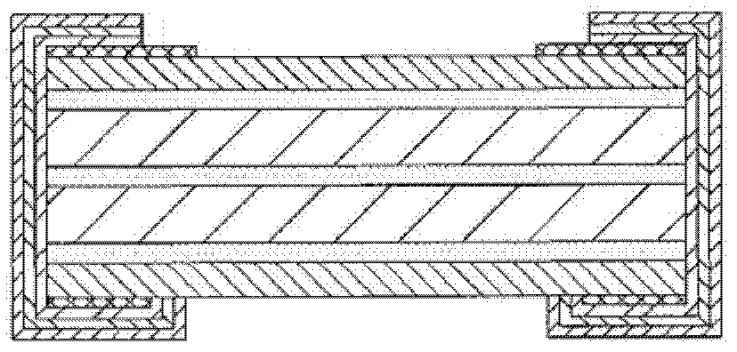
[0073] The inner layer is prepared by setting a sheet-shaped resistance alloy L6 and a sheet-shaped heat-conducting metal L7 on both sides of a piece of insulating heat-conducting adhesive, such as Figure 8 As shown, in this embodiment, the resistance alloy L6, the heat-conducting metal L7 and the insulating heat-conducting adhesive C5 are closely combined by pressing. The resistance alloy can be a material with a small temperature coefficient of resistance, and the resistivity is not limited; the heat-conducting metal is a metal material with a thermal conductivity greater than or equal to 200W / mK; the insulating heat-conducting adhesive can use a single material with good heat resistance, insulation, Thermally conductive, adhesive high-molecular polymer adhesives, or glass fiber-reinforced high-molecular polymer adhesives with good heat resistance, insulation, thermal conductivity, and adhesive properties. Then make the circuit on the inner layer after pressing, that is, fo...

Embodiment 3

[0081] If the resistance alloy and the heat-conducting metal itself have good rigidity, the following manufacturing methods can be followed:

[0082] Firstly, the resistive body is formed on the resistive alloy by etching, and the heat sink is formed on the thermally conductive metal.

[0083] Then, the finished resistor body and heat sink are made according to the following steps: image 3 The method shown is stacked and pressed, and then slotted and drilled mechanically. Metallize the slotted and drilled parts. The method of metallization can be electroless plating and physical vapor deposition, so that the section of the slotted and drilled holes is first covered with a thin metal conductive layer, and then added by electroplating. Thick, so that the final product can withstand the impact of high current.

[0084] The forming of the outer layer circuit also adopts the method of chemical etching to form the pattern of the heat sink on the outer layer, and the pattern of th...


PUM


Abstract

The invention belongs to the field of precision current sensing elements and particularly relates to a structure of a multi-layer structured precision current sensing element with a radiating layer, and a manufacturing method for the structure. The multi-layer structured precision current sensing element comprises at least one layer of resistor body, two layers of radiating sheets, electrodes, an insulation heat conduction adhesive layer, via holes and a protection layer, wherein an insulation slit is formed between the radiating sheets; the insulation heat conduction adhesive layer is arranged between one metal layer and another metal layer; the electrodes are arranged on two sides of a product; the electrodes are connected with the resistor body and the radiating sheets; a via hole is formed in each electrode; and the via holes are connected with the resistor body and the radiating sheets. In the manufacturing method, the thick resistor body is decomposed into a plurality of thin resistor bodies; the thin resistor bodies are subjected to resistance modification, and alloy sheets are connected in parallel with one another; each resistor body is at least provided with one radiating sheet for radiation, so the radiating property of the product is enhanced greatly; furthermore, a layer of protection layer is covered on the outer layer of the multi-layer structured precision current sensing element. The precision current sensing element is high in practicability.

Description

technical field [0001] The invention belongs to the field of precision current sensing elements, and in particular relates to a structure and a manufacturing method of a precision current sensing element for overcurrent protection. Background technique [0002] As we all know, the size of the resistance is related to three factors, the resistivity of the conductor, the length of the conductor and the cross-sectional area of ​​the conductor. Under the premise that the conductor material is fixed, the resistivity of the conductor remains unchanged. To increase the resistance, the length of the conductor can be increased or the cross-sectional area of ​​the conductor can be decreased. To improve the current resistance of the conductor, there are three ways to reduce the resistance, or to increase the length of the conductor in proportion to the cross-sectional area of ​​the resistance without changing the resistance, or to improve the heat dissipation effect. [0003] Most of...

Claims


Application Information

Patent Timeline
Patent Type & Authority Patents(China)
IPC IPC(8): H01C3/00H01C1/084H01C1/148H01C1/02H01C17/00
Inventor 唐彬杨漫雪南式荣
Owner NANJING SART SCI & TECH DEV
Why Eureka
Try Eureka