CNT (carbon nano tube)-silicon heterojunction solar cell and manufacturing method thereof

A solar cell and silicon heterojunction technology, applied in circuits, photovoltaic power generation, electrical components, etc., can solve the problem of high processing cost of single crystal silicon, reduce the possibility of recombination, speed up separation, and improve conversion efficiency.

Active Publication Date: 2012-03-07
TSINGHUA UNIV
View PDF3 Cites 11 Cited by
  • Summary
  • Abstract
  • Description
  • Claims
  • Application Information

AI Technical Summary

Problems solved by technology

Monocrystalline silicon cells have the highest efficiency, but the processing cost of monocrystalline silicon is high. Therefore, it is partic

Method used


Image

  • CNT (carbon nano tube)-silicon heterojunction solar cell and manufacturing method thereof
  • CNT (carbon nano tube)-silicon heterojunction solar cell and manufacturing method thereof
  • CNT (carbon nano tube)-silicon heterojunction solar cell and manufacturing method thereof

Examples


Embodiment 1

[0027] Embodiment 1, the making of carbon nanotube-silicon heterojunction solar cell

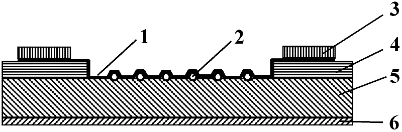
[0028] 1) Prepare SiO with a thickness of 300 nm on the surface of n-type silicon wafer 5 by thermal oxidation 2 thermal oxide layer;

[0029] 2) Using photolithography to etch away the thermal oxide layer on the lower surface of the silicon wafer, and at the same time etch the thermal oxide layer on the central area of ​​the upper surface of the silicon wafer to expose the pure surface of silicon, that is, to obtain a ring-shaped thermal oxide layer covering the upper surface 4 of silicon wafers;

[0030] 3) Evaporate a Ti / Au layer on the lower surface of the silicon wafer to form a good ohmic contact with the lower surface of the silicon wafer as the lower electrode 6, that is, to obtain a Ti / Au layer deposited on the lower surface and a ring-shaped thermal oxide layer deposited on the upper surface Silicon wafer;

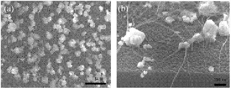
[0031] 4) soak the silicon chip obtained in step 3) in Cu(NO 3 ) 2 Mi...

Embodiment 2

[0035] Embodiment 2, the making of carbon nanotube-silicon heterojunction solar cell

[0036] 1) Prepare SiO with a thickness of 200nm on the surface of n-type silicon wafer by thermal oxidation 2 thermal oxide layer;

[0037] 2) Using photolithography to etch away the thermal oxide layer on the lower surface of the silicon wafer, and at the same time etch the thermal oxide layer on the central area of ​​the upper surface of the silicon wafer to expose the pure surface of silicon, that is, to obtain the upper surface covered with a ring-shaped thermal oxide layer. Silicon wafer;

[0038] 3) Evaporate a Ti / Au layer on the lower surface of the silicon wafer to form a good ohmic contact with the silicon wafer surface as the lower electrode, that is, to obtain a silicon wafer with a Ti / Au layer deposited on the lower surface and a ring-shaped thermal oxide layer deposited on the upper surface ;

[0039] 4) soak the silicon chip obtained in step 3) in Cu(NO 3 ) 2 Mixed aqueous...

Embodiment 3

[0043] Embodiment 3, the making of carbon nanotube-silicon heterojunction solar cell

[0044] 1) Prepare SiO with a thickness of 200nm on the surface of n-type silicon wafer by thermal oxidation 2 thermal oxide layer;

[0045] 2) Using photolithography to etch away the thermal oxide layer on the lower surface of the silicon wafer, and at the same time etch the thermal oxide layer on the central area of ​​the upper surface of the silicon wafer to expose the pure surface of silicon, that is, to obtain the upper surface covered with a ring-shaped thermal oxide layer. Silicon wafer;

[0046] 3) Evaporate a Ti / Au layer on the lower surface of the silicon wafer to form a good ohmic contact with the silicon wafer surface as the lower electrode, that is, to obtain a silicon wafer with a Ti / Au layer deposited on the lower surface and a ring-shaped thermal oxide layer deposited on the upper surface ;

[0047] 4) soak the silicon chip obtained in step 3) in Cu(NO 3 ) 2 Mixed aqueous...


PUM

PropertyMeasurementUnit
Particle sizeaaaaaaaaaa
Thicknessaaaaaaaaaa
Thicknessaaaaaaaaaa

Abstract

The invention discloses a CNT (carbon nano tube)-silicon heterojunction solar cell and a manufacturing method thereof. The solar cell comprises a lower electrode, a silicon wafer arranged on the lower electrode, an annular insulating layer deposited on the silicon wafer, cuprous iodide particles deposited on the silicon wafer and arranged in an annular cavity of the annular insulating layer, a CNT film paved on the insulating layer, the silicon wafer and the cuprous iodide particles, and an annular upper electrode on the CNT. The manufacturing method of the solar cell comprises the following steps of: placing a silicon wafer of which the upper and lower surfaces are provided with the lower electrode and the annular insulating layer in a mixed water solution of Cu (NO3)2 and HF (hydrogen fluoride) to carry out etching so as to obtain a silicon wafer of which the surface is provided with copper particles; placing the silicon wafer with the copper particles in an iodic ethanol solution to carry out halogenation so as to obtain a silicon wafer of which the surface is provided with the cuprous iodide particles; paving the CNT film on the silicon wafer with the cuprous iodide particles; and depositing the upper electrode on the CNT film to obtain the solar cell.

Description

technical field [0001] The invention relates to a carbon nanotube-silicon heterojunction solar cell and a manufacturing method thereof, belonging to the technical field of solar cells and nanomaterial applications. Background technique [0002] Today, when the world advocates sustainable development, renewable energy has become an issue that everyone pays more and more attention to. As one of the renewable clean energy sources, solar energy has been applied in various fields. Among them, solar cells are widely used, and the current solar cells on the market are mainly monocrystalline silicon cells. Monocrystalline silicon cells have the highest efficiency, but the processing cost of monocrystalline silicon is high. Therefore, it is particularly important to explore a new type of cell that consumes less monocrystalline silicon and has high photoelectric conversion efficiency. [0003] In recent years, nanomaterials have attracted extensive attention due to their excellent p...

Claims


Application Information

Patent Timeline
IPC IPC(8): H01L31/032H01L31/072H01L31/18
CPCY02E10/50Y02P70/50
Inventor 王红光韦进全白曦贾怡李培旭朱宏伟王昆林吴德海
Owner TSINGHUA UNIV
Why Eureka
Try Eureka