BIOS (Basic Input Output System) debugger and debugging method

A debugging method and a debugger technology, which are applied in the detection of faulty computer hardware, etc., can solve the problems of inconvenient testing, increased programming time, time wasting, etc., and achieve the effect of high speed and low testing cost

Inactive Publication Date: 2012-03-21
HONG FU JIN PRECISION IND (SHENZHEN) CO LTD +1
View PDF4 Cites 8 Cited by
  • Summary
  • Abstract
  • Description
  • Claims
  • Application Information

AI Technical Summary

Problems solved by technology

[0003] The disadvantage of this debugging method is that it is a waste of time to remove and put the BIOS chip multiple times.
Due to the increasingly powerful BIOS functions, the capacity of BIOS chips of different computers to be tested is also increasing, and the burning time increases accordingly.
In addition, if the computer to be tested has not reached the stage of turning on the screen display or has a critical failure, and there is no display on the screen, the designer cannot know the stage of POST or cannot determine the fault of the computer to be tested, and needs to use the POST diagnostic card According to the code displayed on the POST diagnostic card, look up the POST code table to know the stage of the POST of the computer under test or the cause and location of the fault, which brings inconvenience to the test and wastes time.

Method used


Image

  • BIOS (Basic Input Output System) debugger and debugging method
  • BIOS (Basic Input Output System) debugger and debugging method
  • BIOS (Basic Input Output System) debugger and debugging method

Examples


Embodiment Construction

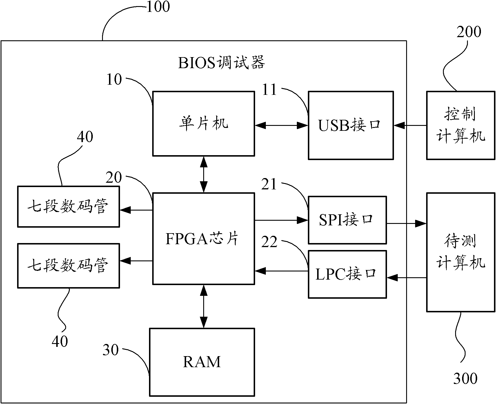
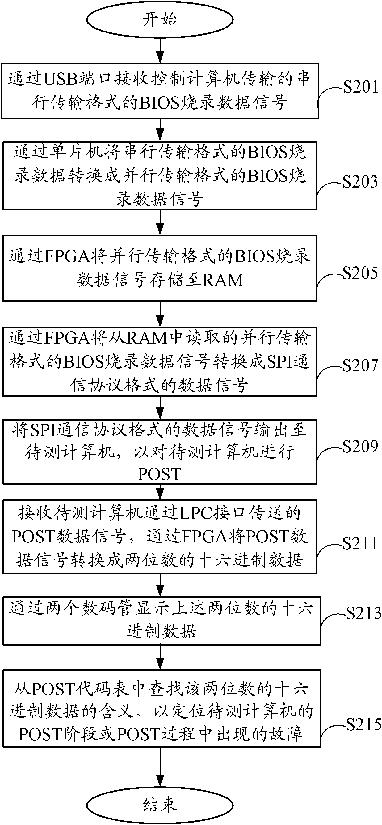
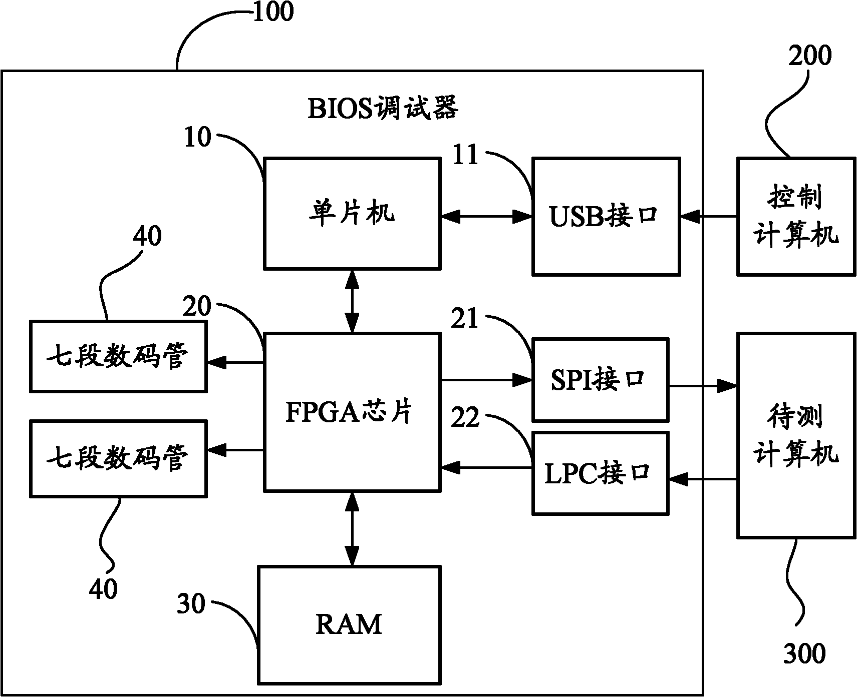
[0012] refer to figure 1 Shown is a functional block diagram of a preferred embodiment of a basic input / output system (BIOS) debugger of the present invention. The BIOS debugger 100 includes a microcontroller 10 , a field-programmable gate array (FPGA) chip 20 , a random access memory (random access memory, RAM) 30 and two seven-segment LEDs 40 . FPGA chip 20 is connected with single-chip microcomputer 10 , RAM 30 and two seven-segment digital tubes 40 . The single-chip microcomputer 10 is connected to the control computer 200 through a universal serial bus (USB) interface 11 , and receives the BIOS programming data signal output by the control computer 200 in a serial transmission format through the USB interface 11 . Afterwards, the microcontroller 10 converts the BIOS programming data signal in the serial transmission format into a BIOS programming data signal in the parallel transmission format to increase the data transmission rate, and outputs the BIOS programming data ...


PUM


Abstract

The invention relates to a BIOS (basic input output system) debugger and a BIOS debugging method. The BIOS debugging method comprises a single chip microcomputer, an FPGA (field programmable gate array) chip, an RAM (random access memory) and two seven-segment digital tubes, wherein the FPGA chip is connected with the single chip microcomputer, the RAM and the two seven-segment digital tubes. BIOS burning data signals in a series transmission format output by a control computer is converted into the BIOS burning data signals in a parallel transmission format to be output to the FPGA chip by the single chip microcomputer. The BIOS burning data signals in the parallel transmission format is stored into the RAM by the FPGA chip, the BIOS burning data signals read in RAM 30 are converted into data signals in an SPI (serial peripheral interface) communication protocol format and then are output to a computer to be tested, so that the POST (power on self test) of the computer to be tested is conducted. The POST data signals output by the computer to be tested are also converted into two-digit hexadecimal data to be output to the two seven-segment digital tubes for displaying.

Description

technical field [0001] The invention relates to a BIOS debugger and a debugging method. Background technique [0002] At present, the method for debugging the BIOS by the basic input / output system (basic input / output system, BIOS) development department mainly includes the following steps: unplug the BIOS chip that needs to be debugged on the computer to be tested, and install the BIOS chip that needs to be debugged on a computer. The computer that works normally, burns the burning data (such as BIOS original file or BIOS update file) to the BIOS chip that needs to be debugged through the burning program. Afterwards, unplug the BIOS chip that needs to be debugged from the computer, insert it back into the computer to be tested, power on the computer to be tested and perform a power on self test (POST), and check whether each component of the computer to be tested works normally . [0003] The disadvantage of this debugging method is that it is a waste of time to remove and...

Claims


Application Information

Patent Timeline
Patent Type & Authority Applications(China)
IPC IPC(8): G06F11/22
Inventor 丛卫东
Owner HONG FU JIN PRECISION IND (SHENZHEN) CO LTD
Why Eureka
Try Eureka