GaN-based ultraviolet detector with p-i-p-i-n structure and preparation method thereof

A p-i-p-i-n, ultraviolet detector technology, applied in the field of ultraviolet detectors, can solve the problems of high avalanche operating voltage, narrow motion path, reduce multiplication factor, etc., and achieve the effect of increased sensitivity, increased multiplication distance, and flexible selection

Active Publication Date: 2012-03-21
TSINGHUA UNIV
View PDF4 Cites 16 Cited by
  • Summary
  • Abstract
  • Description
  • Claims
  • Application Information

AI Technical Summary

Problems solved by technology

In the GaN-based p-i-n type structure, the i-region is responsible for absorbing ultraviolet light and performing two layers of light amplification, which makes it have three defects in the working state: First, if you want to improve the light absorption efficiency, you must increase the thickness of the i-region, which makes The avalanche operatin

Method used


Image

  • GaN-based ultraviolet detector with p-i-p-i-n structure and preparation method thereof
  • GaN-based ultraviolet detector with p-i-p-i-n structure and preparation method thereof
  • GaN-based ultraviolet detector with p-i-p-i-n structure and preparation method thereof

Examples


Embodiment 1

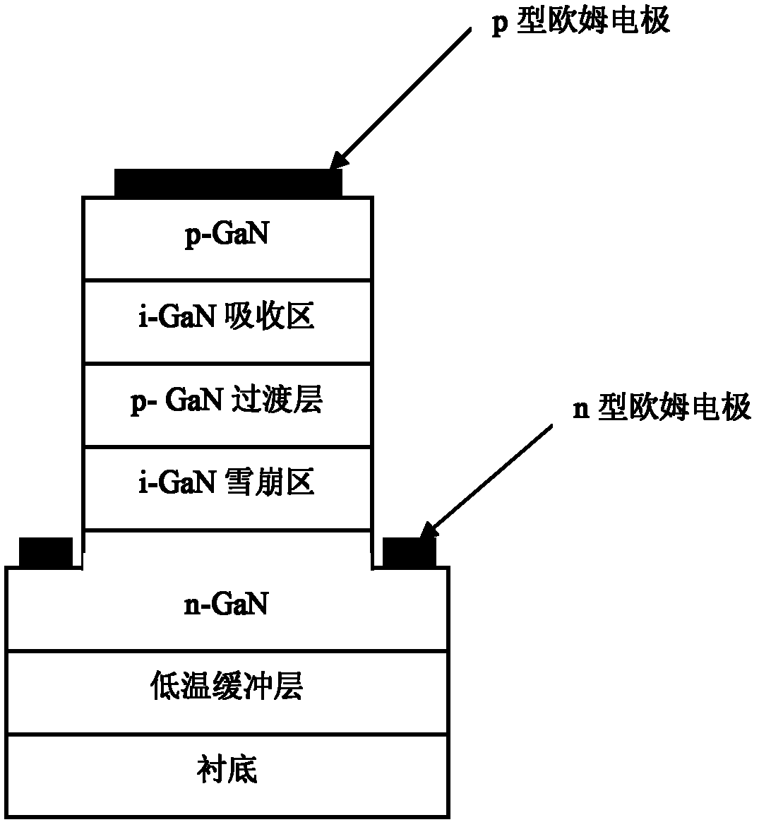
[0035] refer to figure 1 , Embodiment 1 of the present invention provides an avalanche ultraviolet detector with p-i-p-i-n structure of GaN material, which includes substrate sapphire for growing GaN material, n-type GaN low-temperature buffer layer, n-type GaN layer, and i-type GaN multiplication layer , p-type transition layer, i-type GaN photosensitive absorption layer and p-type GaN layer. Its preparation method is as follows:

[0036] (1) Select sapphire as the substrate for growing GaN material.

[0037] (2) Using MOCVD method, trimethylgallium (TMGa) as gallium source, high-purity NH 3 As a nitrogen source, a 20 nm n-type GaN low temperature buffer layer was grown on the above substrate.

[0038] (3) A 3 μm n-type GaN layer is grown on the above buffer layer with a doping concentration of about 5×10 18 cm -3 .

[0039] (4) A 100nm i-type GaN multiplication layer is grown on the n-type GaN layer as an avalanche amplification region for photogenerated carriers (that...

Embodiment 2

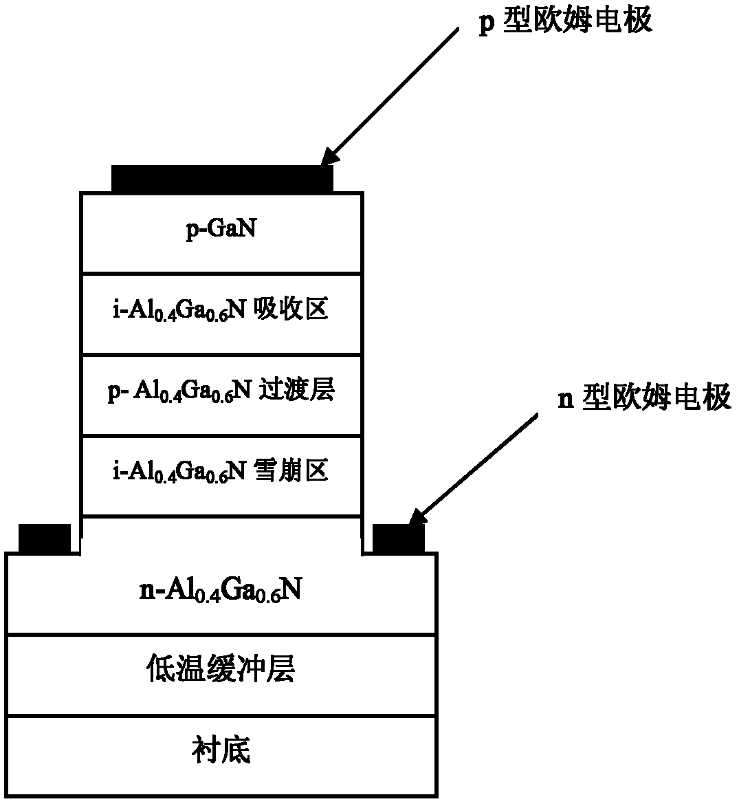
[0047] refer to figure 2 , Embodiment 2 of the present invention provides an Al 0.4 Ga 0.6 An avalanche type ultraviolet detector with p-i-p-i-n structure of N material, which includes a method for growing Al 0.4 Ga 0.6 N-material substrate sapphire, n-type AlN low-temperature buffer layer, n-type Al 0.4 Ga 0.6 N-layer, i-type Al 0.4 Ga 0.6 N multiplication layer, p-type Al 0.4 Ga 0.6 N transition layer, i-type Al 0.4 Ga 0.6 N photosensitive absorption layer and p-type GaN layer. Its preparation method is as follows:

[0048] (1) Select sapphire as the growth Al 0.4 Ga 0.6 N material substrate.

[0049] (2) Using MOCVD method, trimethylgallium (TMGa) as gallium source, high-purity NH 3 As a nitrogen source, a 30 nm n-type AlN low temperature buffer layer was grown on the above substrate.

[0050] (3) Grow a layer of 3 μm n-type Al on the above buffer layer 0.4 Ga 0.6 N layer, the doping concentration is about 5×10 18 cm -3 .

[0051] (4) Grow a layer of 1...


PUM

PropertyMeasurementUnit
Thicknessaaaaaaaaaa
Thicknessaaaaaaaaaa
Thicknessaaaaaaaaaa

Abstract

The invention relates to the technical field of ultraviolet detectors and discloses a GaN-based ultraviolet detector with p-i-p-i-n structure and a preparation method thereof. The detector comprises, from bottom to top, a substrate on which an AlGa<1-x>N material grows, a n-type layer, an i-type Multiplication layer, a p-type transition layer, an i-type photosensitive absorption layer and a p-type layer, wherein x is more than or equal to 0 but less than or equal to 1. The invention has the following two advantages: (1) the design of separation of the multiplication region and the absorption region increases the avalanche multiplication range of current carriers, so as to greatly improve sensitivity; and (2) in the p-i-p-i-n structure, the electric fields are mainly concentrated in themultiplication region, so that the thickness of the absorption region can be increased to increase the absorption efficiency without substantially affecting the selection of a working voltage, as a result, the selection of a working site is more flexible and the applicability of the detector can be improved.

Description

technical field [0001] The invention relates to an ultraviolet detector, in particular to a GaN-based p-i-p-i-n structure ultraviolet detector and a preparation method thereof. Background technique [0002] Ultraviolet detection has a wide range of applications in civilian and military fields, including chemical and biological analysis (ozone, pollutants and most organic compounds have absorption lines in the ultraviolet spectral range), flame detection (including fire alarm, missile early warning and guidance, combustion monitoring etc.), optical communication (especially communication between satellites using ultraviolet light with a wavelength less than 280nm), calibration of ultraviolet light sources (instruments, ultraviolet lithography, etc.), and astronomical research. Traditional ultraviolet detection mainly relies on photomultiplier tubes (PMTs), thermal detectors, narrow-bandgap semiconductor photodiodes or charge-coupled devices (CCDs). PMTs have high gain and lo...

Claims


Application Information

Patent Timeline
IPC IPC(8): H01L31/105H01L31/0352H01L31/18
CPCY02P70/50
Inventor 汪莱郑纪元郝智彪罗毅
Owner TSINGHUA UNIV
Why Eureka
Try Eureka