Low-cost solar cells and methods for fabricating low cost substrates for solar cells
A substrate and wafer technology, applied in the field of battery device structures, can solve the problems of limited availability of pure silicon wafers, low photovoltaic conversion efficiency of thin-film silicon solar cells, and cost constraints, so as to avoid costs, health and environmental hazards, reduce cost, the effect of improving conversion efficiency
- Summary
- Abstract
- Description
- Claims
- Application Information
AI Technical Summary
Problems solved by technology
Method used
Image
Examples
Embodiment 1
[0070] Three nines of metallurgical grade silicon was produced by induction melting two nines of silicon pellets in an approximately 1.5 m x 1.5 m graphite crucible, followed by slow cooling into a cylindrical shape over 24 hours. The carbon-rich surface shell is removed and the cylinders are crushed into grains or granules. The resulting material contains B and P, but is usually p-type with a resistivity in the range of 0.1-1 ohm·cm. The resulting material was then cast into metallurgical grade silicon boles of approximately 0.5m x lm x lm with controlled cooling and dopant adjustment. The block was cut into ingots of 16 square cross-sections with one side slightly larger than 5". Polygonal large grain structure exposed on the backside of the wafer. This produced about 500 metallurgical grade silicon wafers of four-nines and five-nines purity. The wafers were divided into two groups using 4-point probe measurements, the main group having 0.3- Resistivity of 0.5 ohm cm, the ...
Embodiment 2
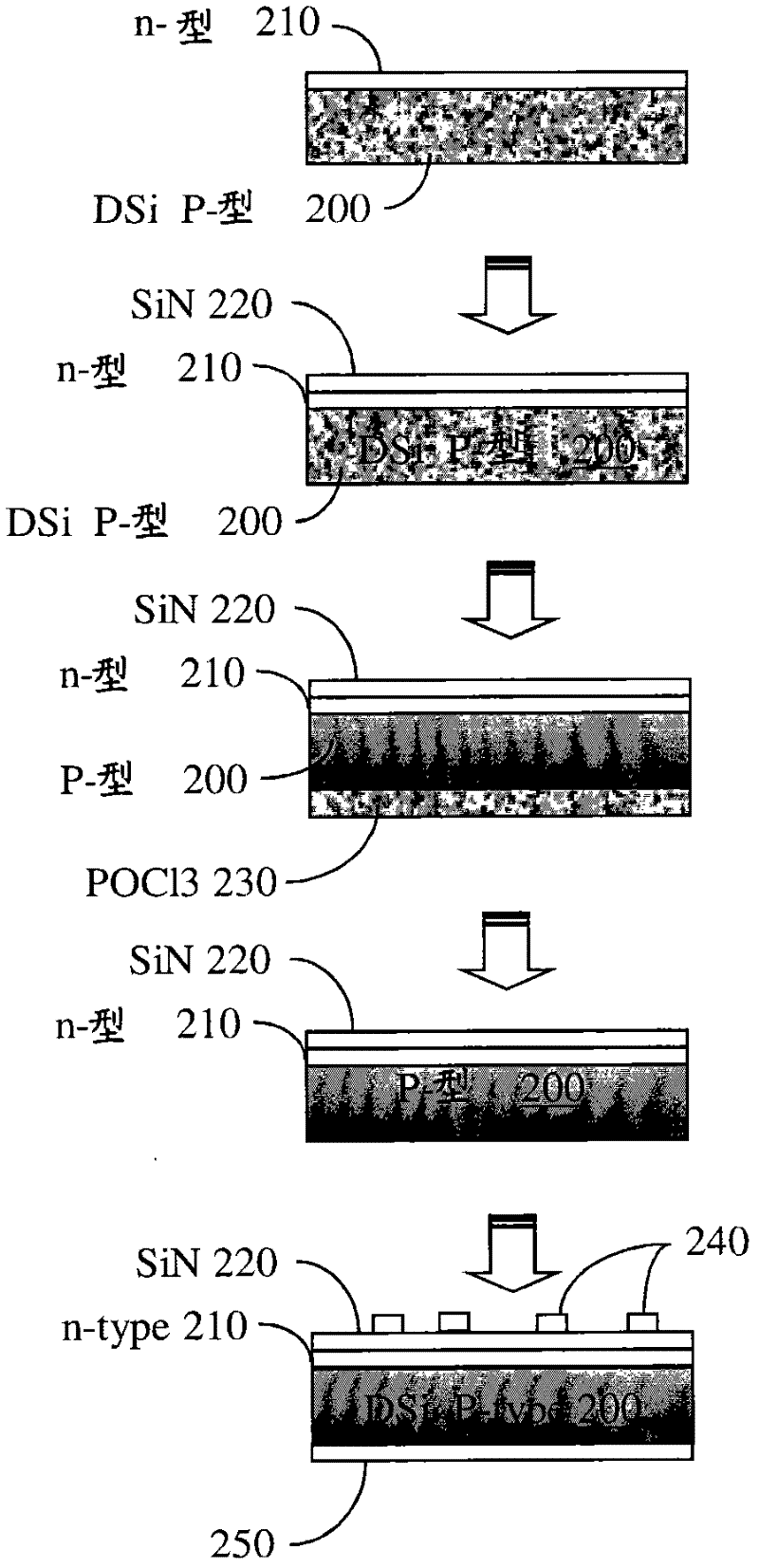
[0073] Formation of intrinsic passivation layers on low-cost metallurgical-grade substrates by depositing nanoscale Si:H film stacks on the front, “device” side and oppositely doped a-Si:H films on the back, “contact” side Single heterojunction for device structures. Metallurgical grade substrates do not have to specifically thin the substrate from 500 μm to 250 μm as is done for crystalline Si substrates, eliminating losses. Thicker wafers provide more robust handling in automated production lines. The material also avoids the cost, cycle, and complexity of polysilicon-based gasification, solidification, melting, and pulling processes, as it passes just outside the metallurgical-grade substrate face passivated by nanoscale intrinsic a-Si:H films thin Si:H films to create the active device.
[0074] Metallurgical grade substrates can be formed in standard sizes such as 6 inches, 8 inches, and 12 inches, and can be processed in standard semiconductor PECVD processing equipmen...
Embodiment 3
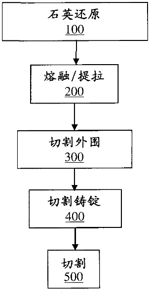
[0076] Figure 9A Instructions are usually referred to in this article as SmartSi TM An example of a process for fabricating a prepared substrate for solar cells. In step 900, metallurgical grade quartz is melted and reduced in an electrolytic cell containing graphite electrodes, then allowed to cool and solidify to provide a metallurgical silicon ingot of about two nines. The ingot is broken into pellets, treated in chemicals to leach surface impurities, and cast into ingots. The ingot is then stripped of its outer shell and broken into three to five nines of metallurgical silicon blocks. The resulting blocks are sorted according to their resistivity.
[0077] In step 915 the sorted MG silicon ingots are cast. The melt is allowed to solidify into bulk, processed in step 920, cut into ingots, and sliced into wafers, eg, 350 microns thick. In addition, each wafer is also etched to remove dicing damage and to clean and prepare the surface of the wafer for further processi...
PUM
 Abstract
Description
Claims
Application Information


