

Method for preparing nanometer structures from top to bottom on surfaces of (110) type silicon chips
A nanostructure and silicon wafer surface technology, which is applied in nanostructure manufacturing, nanotechnology, nanotechnology, etc., can solve the problems of single nanowire structure, high preparation cost, and expensive SOI silicon wafer material, etc., and achieve lattice structure Integrity, good crystal direction alignment and low cost effect
- Summary
- Abstract
- Description
- Claims
- Application Information
AI Technical Summary
Problems solved by technology
Method used
Image

Examples
Embodiment 1
[0034] Design of etched windows on (110) silicon wafers for nanowall structures.
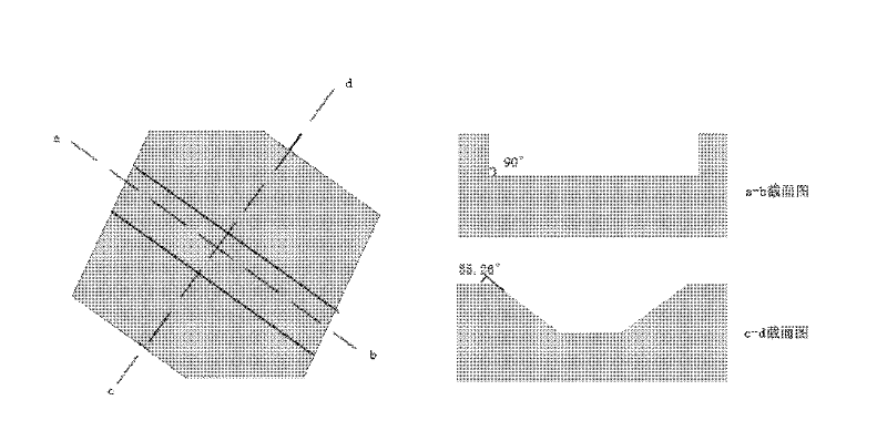
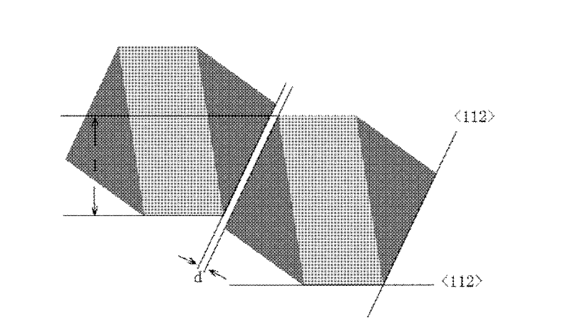
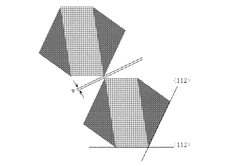
[0035] Assume that the x-axis is along the main cutting edge direction of the (110) type silicon wafer. For simplicity, two identical rectangles are arranged side by side along the x-axis direction, as shown in Figure 5 As shown, the length of the nanowall or nanowire is determined by the projected spacing |a| of the two rectangles on the crystal orientation family at 70.52° to the x-axis. value, a is recorded as the effective side length of the rectangle; the width of the nanowall is only affected by the projection spacing b of the two rectangles on the crystal orientation family with an angle of 160.52° to the x-axis, and has nothing to do with the width of each rectangle. Therefore, as long as the positions of several points of the etching window are determined, nanostructures of the required size can be obtained after anisotropic wet etching, with a width of d, a length of l, and an inclu...
Embodiment 2
[0041] (110) Process flow for preparing single crystal silicon nanowires on a silicon wafer ( Figure 6 ).
[0042] a. Take (110) silicon wafers, after cleaning, high-temperature dry oxygen oxidation of 150nm, as a corrosion protection layer;
[0043] b. Design the etching window according to Example 1, get a=17.5um, b=3um, glue photolithography, BOE removes the silicon oxide in the window;
[0044] c. KOH etching, due to the anisotropic wet etching characteristics of (110) silicon wafers, the original two rectangular windows become two hexagonal etching grooves, and a single crystal silicon of crystal direction is formed in the middle of the two etching grooves The wall structure has a rectangular cross section, the height is determined by the corrosion time, the length and width can be determined by the size and position of the corrosion window, and its width is generally controlled at about 100nm.
[0045] d. High temperature oxidation of 150nm, based on the self-limitin...
Embodiment 3
[0048] A method for preparing single crystal silicon nanostructures on (110) type SOI wafers.
[0049] The method for preparing single-crystal silicon nanostructures on (110) type SOI wafers is basically the same as that of Example 1-2, which can be equivalent to that of Example 1-2 occurring on the top silicon or bottom silicon part of (110) type SOI wafers.
PUM
| Property | Measurement | Unit |
|---|---|---|
| Feature size | aaaaa | aaaaa |
| Thickness | aaaaa | aaaaa |
| Height | aaaaa | aaaaa |
Abstract
Description
Claims
Application Information