

Boron-gallium codoped quasi-monocrystalline silicon and preparation method thereof
A technology of quasi-single-crystal silicon and single-crystal silicon, which is applied in the field of boron-gallium co-doping quasi-single-crystal silicon and its preparation, can solve the problems of reducing the light-induced attenuation of quasi-single-crystal silicon cells, and avoid the loss of boron-oxygen composites. Generate, easy to operate, good stability effect
- Summary
- Abstract
- Description
- Claims
- Application Information
AI Technical Summary
Problems solved by technology
Method used
Image

Examples
Embodiment 1
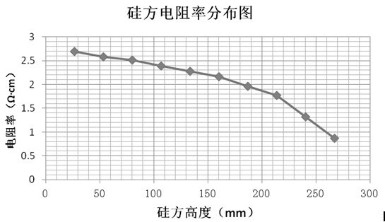
[0031] Cut the single crystal rod in the (100) growth direction into cubes with a section size of 156*156mm and a height of 20mm, and lay them on the bottom of the crucible tightly and orderly. Place silicon raw material on the seed crystal, add 300g of boron-silicon alloy, in which the mass percentage of boron in the borosilicate alloy is about 0.01%, add 1g of metal gallium, a total of about 430kg, and the target resistivity is 1.6Ω·cm . Put the crucible filled with silicon material into the ingot furnace, vacuumize and heat, and control the heater to gradually increase the temperature in the furnace to 1540°C. When the seed crystal starts to melt to the remaining thickness of about 10mm, it jumps from melting to growing crystal stage. In the early stage of crystal growth, quickly lower the temperature from 1540°C to 1440°C, and then start to open the heat shield to make the silicon crystal grow upward from the melting interface of the seed crystal; in the middle stage of c...
Embodiment 2
[0034]Take polysilicon blocks with (100) as the main crystallographic orientation, and lay multiple blocks with a height of 30mm on the bottom of the crucible tightly and orderly. Place silicon raw material on the seed crystal, add 250g of boron alloy and 1g of metal gallium, totaling about 430kg, and target resistivity of 1.6Ω·cm. Put the crucible filled with silicon material into the ingot furnace, evacuate and heat, control the heater to gradually increase the temperature in the furnace to 1530°C, and at the same time adjust the heating rate at the bottom of the crucible to keep the temperature at the bottom of the crucible at 1300°C, so that the seed crystal Partially melted; when the seed crystal starts to melt to about 15mm thick, it jumps from the melting to the growing crystal stage. In the early stage of crystal growth, quickly lower the temperature from 1530°C to 1430°C, and then start to open the heat shield to make the silicon crystal grow upward from the melting i...
Embodiment 3
[0037] Cut the single crystal rod in the (100) growth direction into cubes with a section size of 156*156mm and a height of 10mm, and lay them on the bottom of the crucible tightly and orderly. Place silicon raw material on the seed crystal, add 150g of boron alloy and 4.5g of metal gallium, totaling about 430kg, and target resistivity of 1.7Ω·cm. Put the crucible filled with silicon material into the ingot furnace, evacuate and heat, control the heater to gradually increase the temperature in the furnace to 1550°C, and at the same time adjust the heating rate at the bottom of the crucible to keep the temperature at the bottom of the crucible at 1350°C, so that the seed crystal Partial melting, when the seed crystal starts to melt to about 5mm thick, it jumps from the melting to the growing crystal stage. In the early stage of crystal growth, quickly lower the temperature from 1550°C to 1450°C, and then start to open the heat shield to make the silicon crystal grow upward from...
PUM
| Property | Measurement | Unit |
|---|---|---|
| Resistivity | aaaaa | aaaaa |
| Resistivity | aaaaa | aaaaa |
Abstract
Description
Claims
Application Information