

Through silicon via (TSV) filling method
A filling method and technology of through-silicon vias, which are applied in electrical components, semiconductor/solid-state device manufacturing, circuits, etc., can solve problems such as high cost and complex process, and achieve the effect of reducing process difficulty and cost
- Summary
- Abstract
- Description
- Claims
- Application Information
AI Technical Summary
Problems solved by technology
Method used
Image

Examples
Embodiment Construction
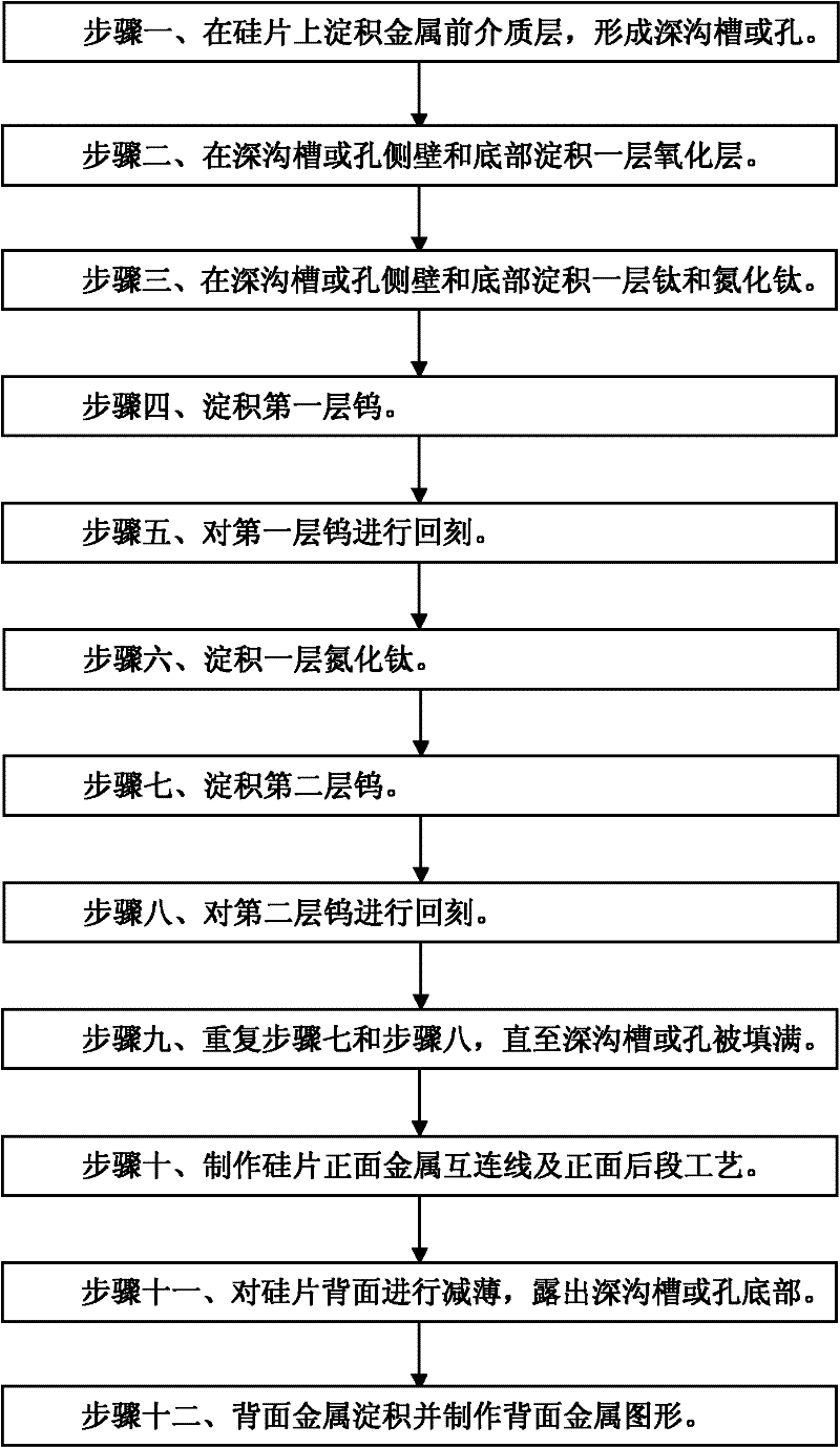
[0034] Such as figure 1 Shown is the flow chart of the embodiment of the present invention. Such as Figure 2 to Figure 12 Shown is a schematic cross-sectional view of a silicon wafer during the manufacturing process of the method of the embodiment of the present invention. The method for filling through-silicon vias according to the embodiment of the present invention includes the following steps:
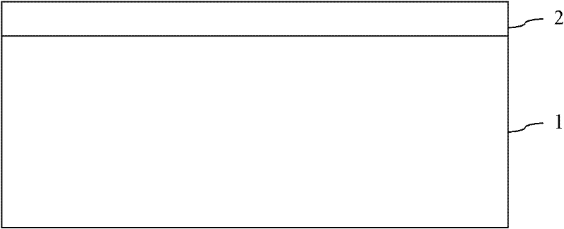
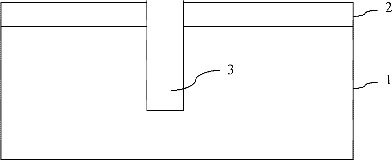
[0035] Step 1, such as figure 2 As shown, a pre-metal dielectric layer 2 is deposited on a silicon wafer 1 . Such as image 3 As shown, a through-silicon hole area is defined by photolithography, and the pre-metal dielectric layer 2 and the silicon wafer 1 in the through-silicon hole area are sequentially etched to form a deep trench or hole 3; the deep trench Or the depth of the hole 3 is 30 microns to 250 microns, preferably 50 microns to 100 microns, and the width is 1.5 microns to 5 microns, most preferably 2 microns to 3 microns; the metal front dielectric layer 2 is bo...
PUM
| Property | Measurement | Unit |
|---|---|---|
| Depth | aaaaa | aaaaa |
| Width | aaaaa | aaaaa |
Abstract
Description
Claims
Application Information