VDMOS (Vertical Double-Diffusion Metal-Oxide-Semiconductor) device with non-uniform floating island structure

A non-uniform, floating island technology, applied in the direction of semiconductor devices, electrical components, circuits, etc., can solve the problems of VDMOS device application limitations, poor reverse recovery characteristics of body diodes, and high manufacturing process difficulty, and achieve good reverse recovery characteristics , large process tolerance and low on-resistance

Inactive Publication Date: 2012-04-18
UNIV OF ELECTRONIC SCI & TECH OF CHINA +1
View PDF5 Cites 20 Cited by
  • Summary
  • Abstract
  • Description
  • Claims
  • Application Information

AI Technical Summary

Problems solved by technology

Due to the constraint relationship between on-resistance and breakdown voltage in traditional VDMOS (on-resistance is proportional to the 2.5th power of breakdown voltage), researchers have proposed to introduce a super-junction structure (super-junction) into the drift region of ordinary VDMOS devices to Optimizing the trade-off

Method used


Image

  • VDMOS (Vertical Double-Diffusion Metal-Oxide-Semiconductor) device with non-uniform floating island structure
  • VDMOS (Vertical Double-Diffusion Metal-Oxide-Semiconductor) device with non-uniform floating island structure
  • VDMOS (Vertical Double-Diffusion Metal-Oxide-Semiconductor) device with non-uniform floating island structure

Examples


Embodiment Construction

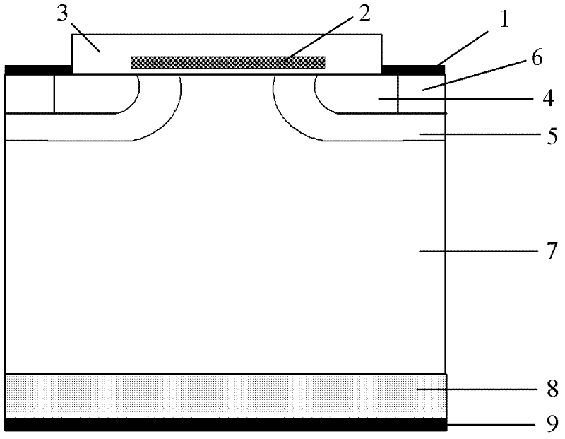
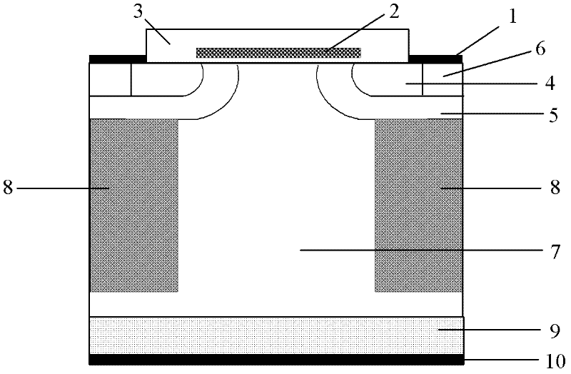
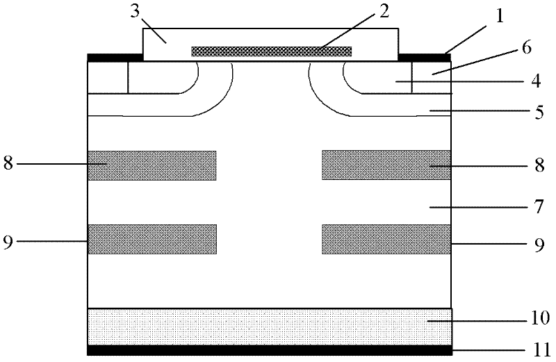
[0026] A VDMOS device with a non-uniform floating island structure, such as Figure 4 As shown, it includes a metallized source electrode 1, a polysilicon gate electrode 2, an insulating dielectric layer 3, a first conductivity type semiconductor doped source region 4, a second conductivity type semiconductor base region 5, and a second conductivity type semiconductor doped contact region 6 , a drift region 7 doped with a semiconductor of the first conductivity type, a substrate 10 doped with a semiconductor of the first conductivity type, and a metallized drain electrode 11 . The metallized drain electrode 11 is located on the back side of the first conductivity type semiconductor doped substrate 10, and the first conductivity type semiconductor doped drift region 7 is located on the front side of the first conductivity type semiconductor doped substrate 10; the second conductivity type semiconductor base region 5 is located on both sides of the top of the first conductivity ...


PUM


Abstract

A VDMOS (Vertical Double-Diffusion Metal-Oxide-Semiconductor) device with a non-uniform floating island structure belongs to the technical field of semiconductor power. For the VDMOS device, the non-uniform floating island structure is drawn into a first conductive type semiconductor drift region of a common VDMOS and comprises at least two layers of second conductive type semiconductor floating islands which are respectively an upper layer of second conductive type semiconductor floating island and a lower layer of second conductive type semiconductor floating island, wherein the upper layer of second conductive type semiconductor floating island is larger in transverse width dimension and lower in doping density, and the lower layer of second conductive type semiconductor floating island is smaller in transverse width dimension and higher in doping density. Compared with the common VDMOS, the VDMOS with the non-uniform floating island, provided by the invention, can adopt higher electrical resistivity of an epitaxial layer under the condition the same puncture voltage, thereby the on-resistance is greatly reduced; compared with a VDMOS with a uniform floating island, the VDMOS with the non-uniform floating island is wider in current path and also can lead the on-resistance to be reduced; and compared with a super-junction VDMOS, the VDMOS is better in the reverse recovery characteristic of a body diode and is relatively simple in process.

Description

technical field [0001] The invention belongs to the technical field of power semiconductor devices, and relates to a vertical double diffusion metal-oxide-semiconductor field effect transistor (Vertical Double Diffusion MOSFET, VDMOS), especially a VDMOS device with a floating island structure. Background technique [0002] VDMOS devices have many advantages such as high input impedance, fast switching speed, voltage drive, and good thermal stability, so they are widely used in power systems. In switching device applications, it is generally desired that VDMOS not only have a high breakdown voltage, but also have a low on-resistance to reduce power consumption, and at the same time have good body diode reverse recovery characteristics to suppress noise and voltage surges during switching . Due to the constraint relationship between on-resistance and breakdown voltage in traditional VDMOS (on-resistance is proportional to the 2.5th power of breakdown voltage), researchers ha...

Claims


Application Information

Patent Timeline
IPC IPC(8): H01L29/78H01L29/06
Inventor 任敏李泽宏邓光敏张灵霞张金平张波
Owner UNIV OF ELECTRONIC SCI & TECH OF CHINA
Why Eureka
Try Eureka