
Method for spraying cracked selenium source on surface of substrate

A substrate surface, selenium source technology, applied in gaseous chemical plating, coating, electrical components, etc., can solve the problems of reducing material utilization, loss of indium and gallium elements, poor reactivity, etc., to improve photoelectric conversion efficiency , Improve the quality of film formation, improve the effect of reactivity

Inactive Publication Date: 2012-05-02
CHINA ELECTRONIC TECH GRP CORP NO 18 RES INST
View PDF1 Cites 9 Cited by
  • Summary
  • Abstract
  • Description
  • Claims
  • Application Information

AI Technical Summary

Problems solved by technology

However, the vapor pressure of selenium is difficult to control, and the gaseous selenium is often represented by Se n (n≥5) Large atomic groups exist in the form of poor reactivity, which can easily lead to insufficient compounding reaction of selenium element, causing loss of indium and gallium elements, reducing material utilization and causing CIGS thin film composition to deviate from ideal stoichiometric ratio, reducing Film quality of CIGS layer

Method used


Image

  • Method for spraying cracked selenium source on surface of substrate
  • Method for spraying cracked selenium source on surface of substrate
  • Method for spraying cracked selenium source on surface of substrate

Examples


Embodiment 1

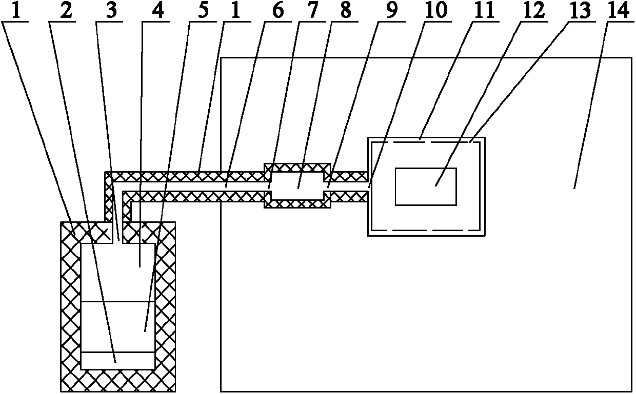
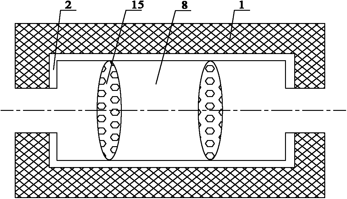
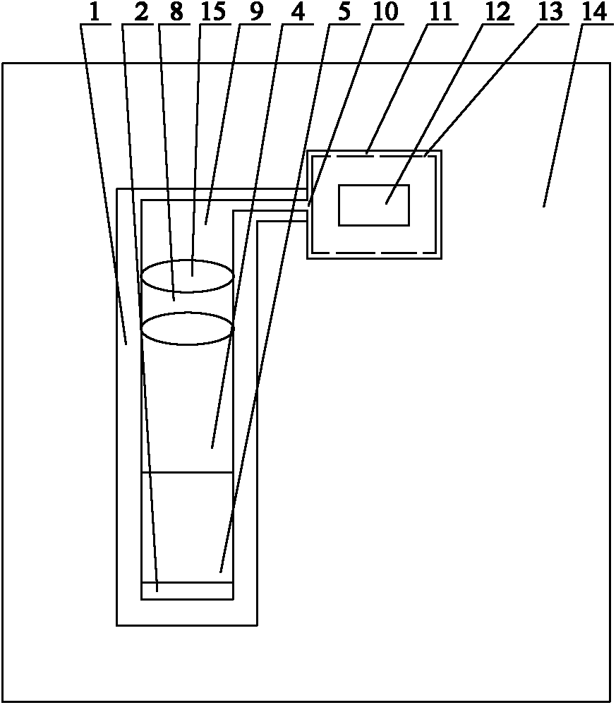
[0024] Refer to attached figure 1 , figure 2 , a method for spraying and cracking a selenium source on the surface of a large-area roll-to-roll flexible substrate, the steps are:

[0025] ⑴ Preparatory work for cracking selenium source:

[0026] Prepare the selenium source evaporation chamber 4, the high temperature cracking chamber 8, the vacuum chamber 14 and the gas outlet pipeline 11 respectively;

[0027] A stainless steel barrel with a volume greater than 1L is selected as the selenium source evaporation chamber, and a small opening on the selenium source evaporation chamber is used as the steam outlet 3. A temperature control heater 2 is arranged at the bottom of the selenium source evaporation chamber, and the solid selenium 5 is located at the temperature control heater. Above; select a stainless steel channel as the high-temperature cracking chamber, one end of the high-temperature cracking chamber is the cracking chamber inlet 7, and the other end is the cracking...


PUM

PropertyMeasurementUnit
pore sizeaaaaaaaaaa

Abstract

The invention relates to a method for spraying a cracked selenium source on the surface of a substrate. The method comprises the following steps: entering selenium steam into a high-temperature cracking chamber; penetrating the selenium steam through two layers of porous grid plates with uniformly distributed pores, the pore diameter of which is 0.2-0.5mm, in the high-temperature cracking chamber, so that the selenium source forms cracked selenium source; and spraying the cracked selenium source to the surface of the substrate so as to complete the process of spraying the cracked selenium source on the surface of the substrate. According to the method provided by the invention, the selenium steam is adopted to penetrate through the two layers of porous grid plates at high temperature, and a large Sen (n is more than or equal to 5) atomic cluster is cracked to form a small Sen (n is less than 5) atomic cluster, thereby increasing the quantity of high-activity Se2, improving the reaction activity of a selenium element, effectively improving the film-forming quality of a CIGS (copper indium gallium selenium) layer of a CIGS film solar battery and taking an positive effect on improvement of photoelectric conversion efficiency of the CIGS film solar battery; and the selenium steam with the small atomic cluster is directly sprayed to the surface of the substrate through spray orifices, so that a selenium material can sufficiently participate in the reaction film-forming process of the CIGS layer, thereby improving the utilization rate of the selenium material.

Description

technical field [0001] The invention belongs to the technical field of copper indium gallium selenium thin film solar cells, in particular to a method for spraying and cracking selenium sources on the surface of a substrate. Background technique [0002] Copper indium gallium selenide thin-film solar cells are one of the most promising thin-film solar cells at present. They have the advantages of high conversion efficiency, no light-induced degradation, good radiation resistance, low cost, and are suitable for large-scale production of roll-to-roll processes. The typical structure is: metal back electrode Mo layer, absorption layer CIGS layer, buffer layer CdS, window layer high resistance i:ZnO, low resistance ZnO:Al, MgF 2 Anti-reflection film and Ni-Al gate electrode, the preparation of absorbing layer CIGS layer is the core technology of copper indium gallium selenide thin film solar cell. [0003] Multivariate co-evaporation is the most widespread and successful method...

Claims


Application Information

Patent Timeline
Patent Type & Authority Applications(China)
IPC IPC(8): C23C16/455C23C16/22H01L31/18
CPCY02P70/50
Inventor 张颖武赵彦民乔在祥
Owner CHINA ELECTRONIC TECH GRP CORP NO 18 RES INST
Learn More