


Quick Research
Generate reliable direction feasibility study reports for your R&D in just a few steps.

Technical Q&A
Discover and master advanced knowledge NOW. Basics, ideas, possibilities, all at once.

Find Solutions
As an expert in R&D theories, this can generate solutions to your technical problems instantly.

Evaluate Feasibility
Analyze your overall solution with one click, know your potential R&D risks in advance.

Monitor Landscape
Get weekly tech updates, stay abreast of the latest tech innovations and key insights.
Method for preparing nanoimprint template
A nano-imprinting and template technology, which is applied to the photoplate making process of the pattern surface, optical mechanical equipment, instruments, etc., can solve the problems of failed pattern transfer, inability to realize large-area pattern transfer, and limited application, so as to meet the requirements of large-scale Industrial production, realization of large-area high-precision graphics transfer, simple and convenient production process
- Summary
- Abstract
- Description
- Claims
- Application Information
AI Technical Summary
Problems solved by technology
Method used
Image

Examples
Embodiment 1
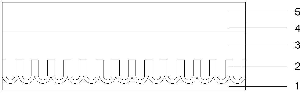
[0031] 1. Rinse the PAT with deionized water repeatedly for 3 to 5 times, and then wash it with N 2 Blow dry with an air gun and bake on the surface of a hot plate at 60°C for 10 minutes. The PAT includes a porous oxide layer and an Al base layer as figure 1 As shown in 2 and 1, the microstructure pattern parameters are: pore depth ~ 600nm, pore diameter ~ 500nm, pore spacing ~ 800nm;
[0032] 2. Spin-coat a layer of photoresist ( figure 1 In 3), this embodiment is preferably SU8-25 series photoresist, and its spin coating parameters are step1: 500r 10s, step2: 2300r 30s. Then bake on a hot plate, the baking parameters are step1: 75°C for 3 minutes, step2: 105°C for 7 minutes. Then stick a layer of double-sided adhesive ( figure 1 In 4), the double-sided adhesive tape is transparent to ultraviolet rays and has strong adhesion. Then the other side of the above-mentioned double-sided adhesive is adhered to quartz glass ( figure 1 Middle 5) The surface is subjected to embos...
Embodiment 2
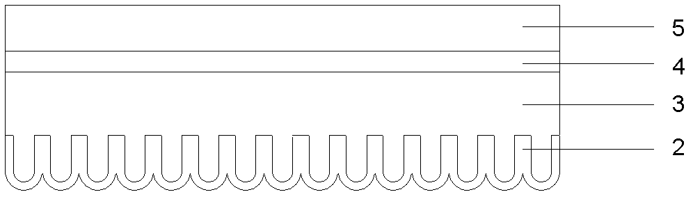
[0038] 1. Rinse the PAT with deionized water repeatedly for 3 to 5 times, and then wash it with N 2 Blow dry with an air gun and bake on the surface of a hot plate at 60°C for 10 minutes, then use perfluorooctyltrichlorosilane CF 3 (CF 2 ) 5 (CH 2 ) 2 SiCl 3 or perfluoroquinyltrichlorosilane CF 3 (CF 2 ) 7 (CH 2 ) 2 SiCl 3 Silane molecules containing Si≡X (wherein X is a halogen element) chemical bond are self-assembled on the surface of the PAT by a single-molecule anti-adhesive layer by vacuum heating and volatilization deposition. The pattern parameters of the PAT microstructure are the same as in Example 1. The method of making the self-assembled monomolecular anti-adhesive layer adopted in this embodiment may also be a liquid-phase self-assembled anti-adhesive method;
[0039] 2. Spin-coat a layer of SU8-2 series photoresist ( figure 1 In 3), the spin coating parameters are step1: 500r 10s, step2: 2000r 30s. Then bake on a hot plate, the baking parameters ar...
PUM
| Property | Measurement | Unit |
|---|---|---|
| Hole depth | aaaaa | aaaaa |
| Aperture | aaaaa | aaaaa |
| Spacing | aaaaa | aaaaa |
Abstract
Description
Claims
Application Information
 - R&D Engineer
- R&D Manager
- IP Professional
- Industry Leading Data Capabilities
- Powerful AI technology
- Patent DNA Extraction
Browse by: Latest US Patents, China's latest patents, Technical Efficacy Thesaurus, Application Domain, Technology Topic, Popular Technical Reports.
© 2024 PatSnap. All rights reserved.Legal|Privacy policy|Modern Slavery Act Transparency Statement|Sitemap|About US| Contact US: help@patsnap.com