Power MOSFET (metal-oxide-semiconductor field effect transistor) device and manufacturing method thereof

A power and device technology, which is applied in the field of power MOSFET devices, can solve the problems of limited space for reducing the manufacturing cost of MOS devices, and achieve the effects of reducing the width, reducing the overall area, and saving size

Inactive Publication Date: 2012-05-02
WUXI NCE POWER
View PDF6 Cites 12 Cited by
  • Summary
  • Abstract
  • Description
  • Claims
  • Application Information

AI Technical Summary

Problems solved by technology

[0004] Such as attached in Chinese patent ZL 200710302461.4 Figure 4 As shown, the terminal protection area of ​​the device includes at least one guard ring located in the inner ring and a stop ring located in the outer ring, and the stop ring includes a trench-type stop ring and a P well located outside the trench layer or a P well layer with an N+ implanted region above, and the stop ring occupies 30%-40% of the width of the entire terminal protection area. Therefore, if the trench power MOS device and its manufacturing method, then the MOS device manufacturing cost reduction space will be very limited

Method used


Image

  • Power MOSFET (metal-oxide-semiconductor field effect transistor) device and manufacturing method thereof
  • Power MOSFET (metal-oxide-semiconductor field effect transistor) device and manufacturing method thereof
  • Power MOSFET (metal-oxide-semiconductor field effect transistor) device and manufacturing method thereof

Examples


Embodiment Construction

[0055] The present invention will be further described below in conjunction with specific drawings and embodiments.

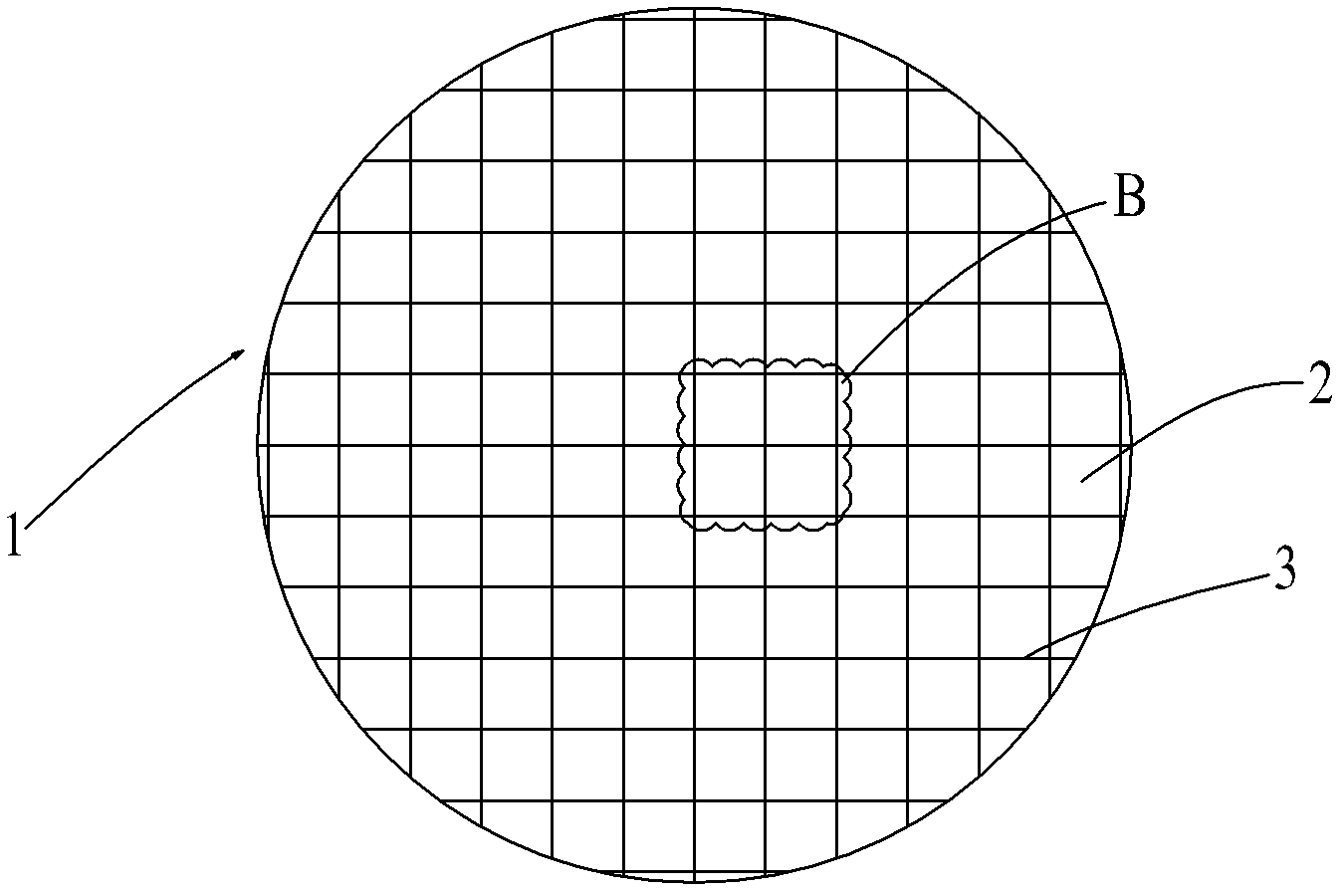
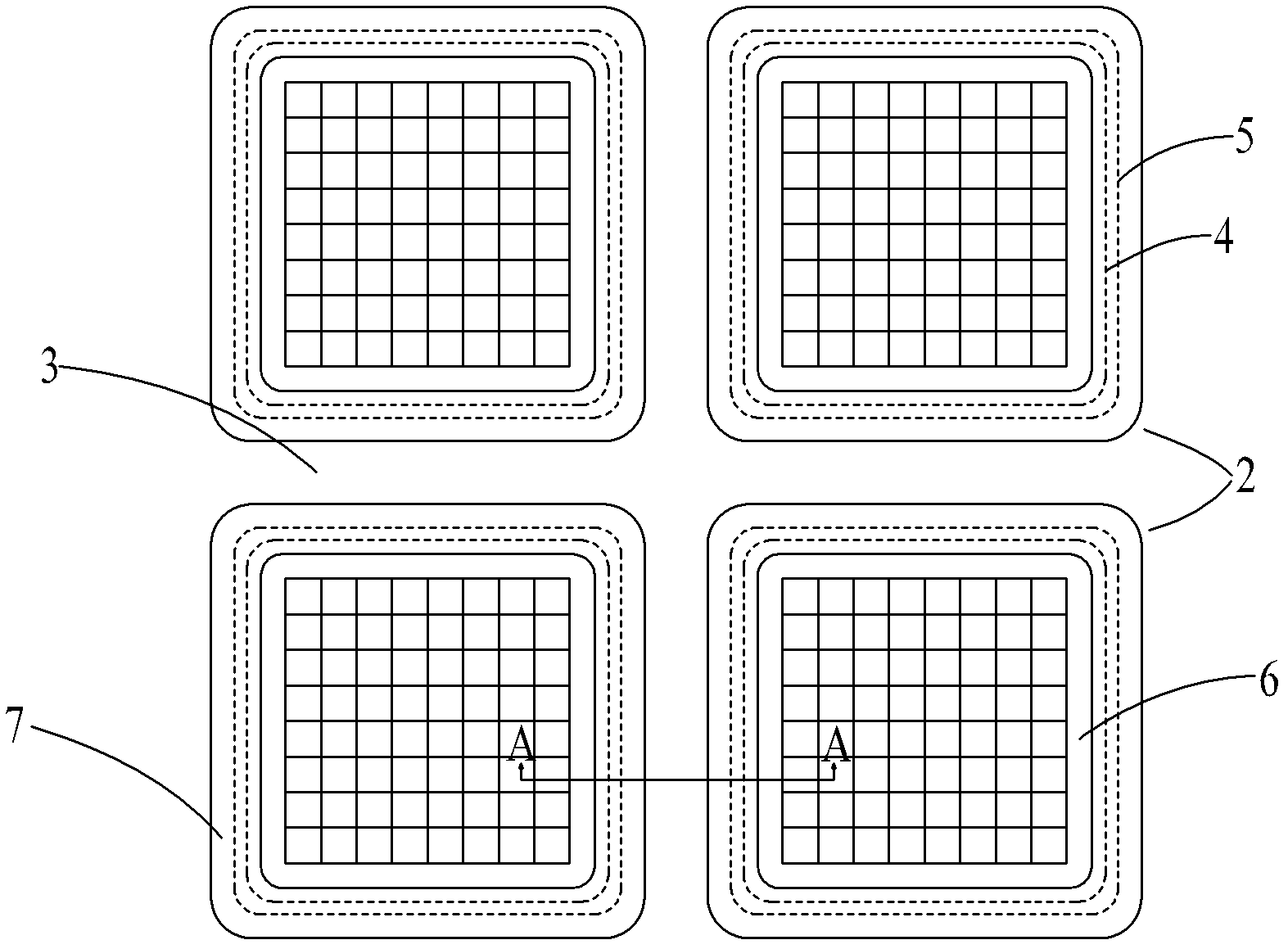
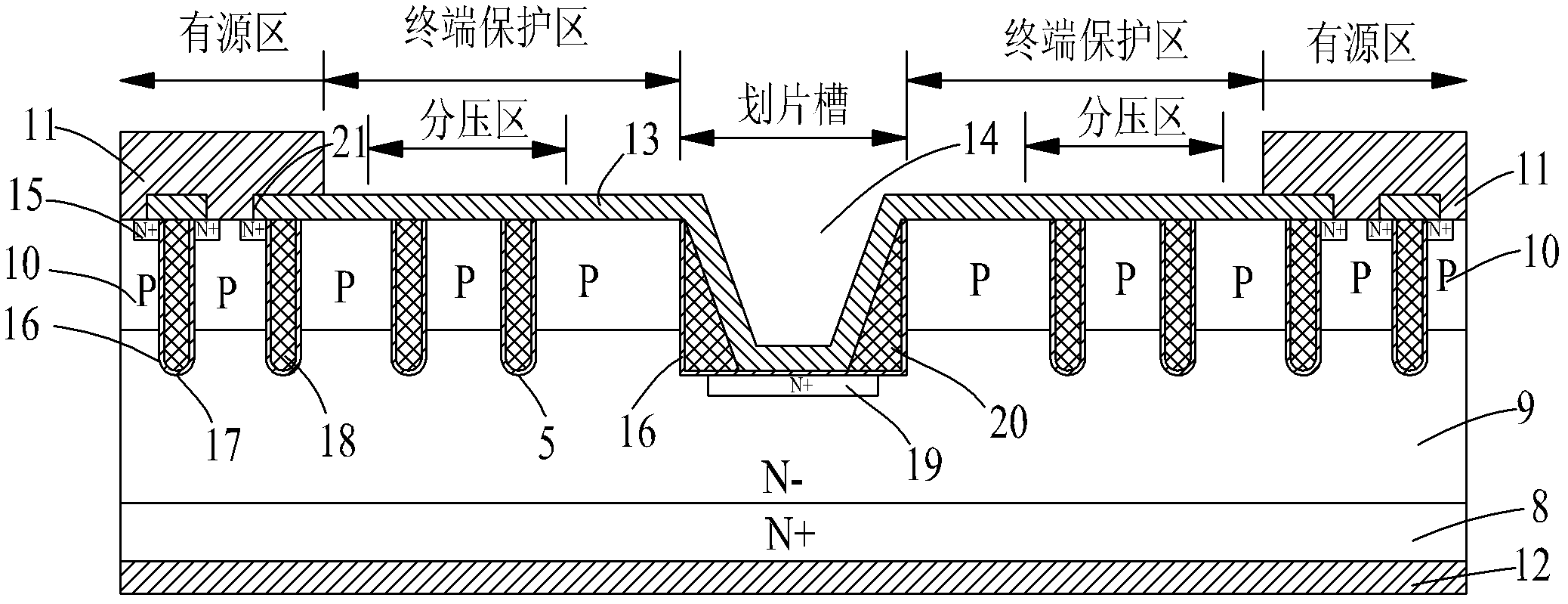
[0056] Such as Figure 1~Figure 13 As shown: taking the N-type power MOSFET device adopting the trench structure as an example, the present invention includes a semiconductor substrate wafer 1, a power MOSFET device 2, a dicing groove 3, a voltage divider ring 4, a voltage divider ring groove 5, an active Region 6, terminal protection region 7, N+ substrate 8, N-type drift region 9, P well layer 10, source metal 11, drain metal 12, insulating dielectric layer 13, scribe groove groove 14, N+ implantation region 15 , insulating gate oxide layer 16, cell trench 17, conductive polysilicon 18, N-type trench step implantation region 19, conductive polysilicon sidewall 20, ohmic contact hole 21, hard mask layer 22, hard mask layer opening 23 and Dicing groove groove step 24 .

[0057] Such as figure 1 As shown, on the top view plane of the semiconductor substrate ...


PUM


Abstract

The invention relates to a power MOSFET (metal-oxide-semiconductor field effect transistor) device and a manufacturing method thereof. The power MOSFET device comprises an active region and a terminal protecting region which are arranged on a semiconductor substrate. On the vertical view plane of the power MOSFET device, a scribing slot trench step is arranged in the scribing slot of the outer ring of the terminal protecting region; insulating gate oxidation layers cover the side wall and bottom of the scribing slot trench step, and a conducting polysilicon side wall is deposited on the scribing slot trench step covered with the insulating gate oxidation layers; insulating dielectric layers cover the corresponding insulating gate oxidation layers of the conducting polysilicon side wall and the bottom in the scribing slot trench step, and the insulating dielectric layers are connected with insulating dielectric layers on the terminal protecting region; and a first conducting type trench step injection region is arranged below the bottom of the scribing slot trench step. The power MOSFET device is compact in structure; the manufacturing cost of the MOSFET device is reduced; and the pressure-resistance capacity of the MOSFET device is improved.

Description

technical field [0001] The invention relates to a MOSFET device and a manufacturing method thereof, in particular to a power MOSFET device and a manufacturing method thereof, and belongs to the technical field of power MOSFET devices. Background technique [0002] Trench power MOSFET devices (Trench MOSFET) can usually obtain higher current density per unit area, so it is an important technical choice to improve product cost performance. Reducing the device chip area can effectively reduce the manufacturing cost of the device, but directly reducing the active area of ​​the device will reduce the ability of the device to conduct current, which is not advisable. Then a more compact device that does not affect the withstand voltage performance of the device The terminal protection area structure will have a more competitive cost advantage. [0003] At present, Chinese patent ZL 200710302461.4 discloses "A Deep Trench High-Power MOS Device and Its Manufacturing Method", which r...

Claims


Application Information

Patent Timeline
Patent Type & Authority Applications(China)
IPC IPC(8): H01L29/78H01L29/06H01L21/336
Inventor 朱袁正叶鹏
Owner WUXI NCE POWER
Why Eureka
Try Eureka