Method for manufacturing solar battery photoanode and product thereof

A solar cell, photoanode technology, applied in nanotechnology for material and surface science, final product manufacturing, sustainable manufacturing/processing, etc., can solve the problems of high manufacturing cost, harsh process conditions, complex process equipment, etc. Achieve the effect of rapid synthesis, simple equipment and mild preparation conditions

Inactive Publication Date: 2012-05-09
HUAZHONG UNIV OF SCI & TECH
View PDF2 Cites 27 Cited by
  • Summary
  • Abstract
  • Description
  • Claims
  • Application Information

AI Technical Summary

Problems solved by technology

However, these methods have the following defects: complex process equipment, harsh process conditions, high manufacturing costs, and are not conducive to mass production

Method used


Image

  • Method for manufacturing solar battery photoanode and product thereof
  • Method for manufacturing solar battery photoanode and product thereof
  • Method for manufacturing solar battery photoanode and product thereof

Examples


Embodiment 1

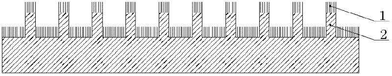
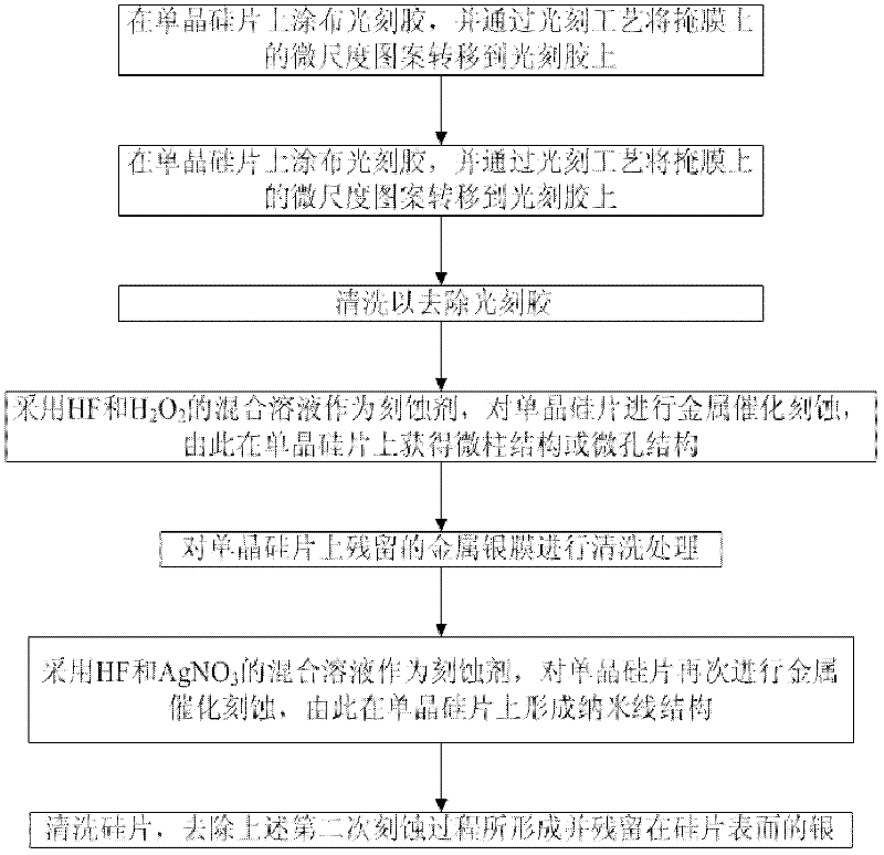
[0030] see figure 1 and image 3 , figure 1 It is a schematic diagram of the product structure prepared according to Embodiment 1 of the present invention, image 3 is a process flow block diagram of the manufacturing method according to the present invention. Such as image 3 and figure 1 Shown in, the method for manufacturing solar cell photoanode in the present embodiment comprises the following specific steps:

[0031] (a) Spin-coat AZ5214 photoresist on the monocrystalline silicon wafer as the photoanode substrate of the solar cell after surface cleaning treatment, and make the micro-scale pattern on the mask, that is, the structure in the order of microns, by photolithography The pattern is transferred to the photoresist, thereby forming the photoresist pattern of the microcolumn array; the microcolumn array here is a micron-scale columnar array structure;

[0032] (b) On the monocrystalline silicon wafer formed with the above-mentioned microcolumn array, adopt a s...

Embodiment 2

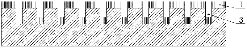
[0040] see figure 2 and image 3 , figure 2 It is a schematic diagram of the product structure obtained according to Embodiment 2 of the present invention. Its specific manufacturing process includes:

[0041] (a) AZ5214 photoresist is coated on the single crystal silicon wafer after surface cleaning, and the micro-scale pattern on the mask is transferred to the photoresist by photolithography process. The photoresist pattern is a microhole array That is, micron-scale hole array structure;

[0042] (b) Coating a 30nm silver film on the entire monocrystalline silicon wafer by a magnetron sputtering process;

[0043] (c) Use acetone to ultrasonically clean the silicon wafer for 10 minutes to remove the photoresist;

[0044] (d) using hydrogen fluoride and H 2 o 2 The mixed solution is used as an etchant to perform metal-catalyzed etching on a single crystal silicon wafer, thereby corroding a silicon micropore array structure, that is, a micron-scale micropore array stru...


PUM


Abstract

The invention discloses a method for manufacturing a solar battery photoanode and a product thereof. The method comprises the following steps of: firstly, coating a photoresist on a monocrystalline silicon wafer and transferring a micro-scale design on a mask through photoetching; secondly, plating a silver film through a film plating process; thirdly, cleaning to remove the photoresist; fourthly, carrying out metal catalytic etching by adopting mixed solution of hydrogen fluoride and H2O2 as an etchant to form a microcolumn or micropore structure; fifthly, cleaning the metallic silver film remained on the monocrystalline silicon wafer; sixthly, carrying out metal catalytic etching again by adopting mixed solution of hydrogen fluoride and AgNO3 as an etchant to form a nanometer line structure; and seventhly, cleaning the silicon wafer, removing silver formed and remained on the surface of the silicon wafer during the second etching process. According to the invention, a micro-nanometer structure combined with a manometer line and a micropore or a microcolumn array can be obtained; and the method disclosed by the invention has the characteristics of high efficiency and low cost andis suitable for the batch production of solar batteries.

Description

technical field [0001] The invention relates to the field of micro-nano processing, more specifically, to a method for manufacturing a solar photoanode with a micro-nano structure and a product thereof. Background technique [0002] Since nanowires were discovered in the 1990s, they have immediately attracted the attention of scientists all over the world and become a hot topic of extensive research in the world's scientific community. Nanowires are typical one-dimensional nanomaterials. Due to their small-scale effects, quantum size effects, surface effects, and macroscopic quantum tunneling effects, they exhibit different properties from traditional ones in terms of optical, electrical, magnetic, thermal, mechanical, and mechanical properties. Different superior properties of bulk materials. [0003] When nanowires are combined with microstructures, they will exhibit many exotic properties, such as very good light absorption properties, super-hydrophobic properties, etc.,...

Claims


Application Information

Patent Timeline
Patent Type & Authority Applications(China)
IPC IPC(8): H01L31/18H01L31/0224B82Y30/00B82Y40/00
CPCY02P70/50
Inventor 廖广兰盛文军史铁林孙博高阳
Owner HUAZHONG UNIV OF SCI & TECH
Why Eureka
Try Eureka