[0029] In order to fully understand the purpose, features and effects of the present invention, the following specific embodiments are used in conjunction with the accompanying drawings to give a detailed description of the present invention. The description is as follows:
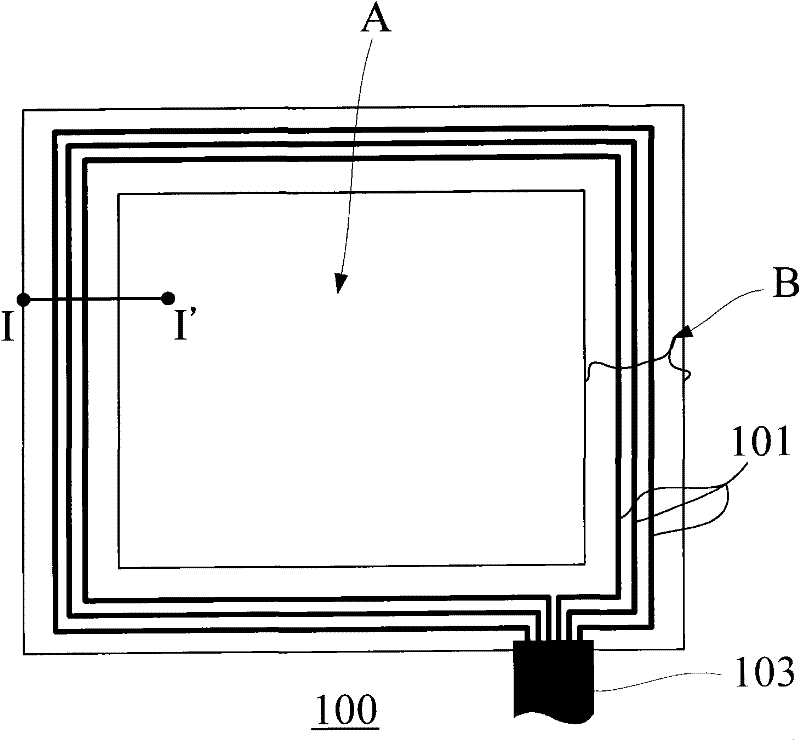
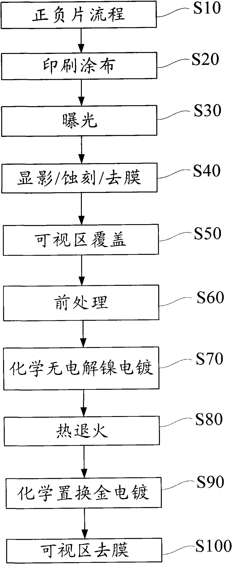
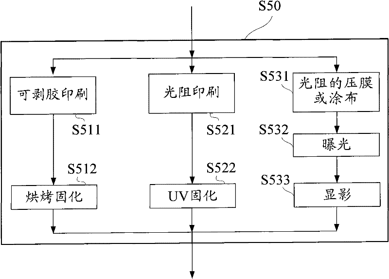
[0030] The low-impedance circuit layer added to the original electronic control circuit of the present invention is different from the low-impedance circuit layer formed by the silver glue printing method, the molybdenum/aluminum/molybdenum sputtering method, and the copper electroplating sputtering method. It is known that the exposure/development/etching process performed in the non-visible area on the substrate makes the transparent conductive layer into an indium tin oxide electronic control circuit. The present invention further carries out the subsequent method steps for reducing the surface resistance of the electronic control circuit. In other words, the present invention adds nickel and gold materials to the indium tin oxide electric control circuit, and the indium tin oxide electric control circuit forms a low impedance electric control circuit, and can reduce the original 100Ω/cm 2 Up to 500Ω/cm 2 The surface resistance value drops to about 3Ω/cm 2.
[0031] See first figure 1 , The schematic diagram of the electrical control circuit on the transparent conductive plate of the general touch panel. figure 1 The transparent conductive plate shown is one of the upper and lower transparent conductive plates in the touch panel. The transparent conductive plate of the other part may have a different substrate, but a transparent conductive indium tin oxide is formed on the substrate. The present invention only exemplifies the production of one transparent conductive plate, and the production of the other is the same. figure 1 In the touch panel, there is a transparent conductive plate 100, which includes a visible area A and an invisible area B. The electronic control circuit 101 is formed in the invisible area B, and the touch action is controlled by the signal cable 103. The generated voltage signal is transmitted. The transparent conductive plate 100 includes a substrate and a transparent conductive layer coated on the substrate. The substrate can be a rigid glass substrate or a soft flexible substrate or a substrate of other properties. The layers are overlapped together, and the visible area A plus the invisible area B in the diagram are superimposed together.
[0032] The present invention firstly completes the production of the indium tin oxide electronic control circuit on the substrate by the well-known circuit manufacturing technology, and then performs the manufacturing method of the low impedance electronic control circuit of the present invention.
[0033] Then see figure 2 , A flowchart of a method for manufacturing a low impedance electronic control circuit in an embodiment of the present invention. There are seven steps in the diagram, among which steps S10 to S40 are an example of the manufacturing steps of the indium tin oxide electric control circuit. For example: Step S10 is the positive and negative film process, and then the printing and coating of step S20 are carried out to pre-lay out the required electrical control circuit traces on the transparent conductive layer, then step S30 will be fully exposed, and the final step S40 will be developed /Etching/Removing the film will complete the production of all indium tin oxide electronic control circuits.
[0034] After the foregoing steps are completed, the surface resistance of the electric control circuit can be further reduced after the following steps and methods proposed by the present invention. Among them, the aforementioned steps are only an example, and any other indium tin oxide electrical control circuit can be manufactured by the present invention.
[0035] Next, the visible area covering step of step S50 is performed, which is used to cover the visible area with a protective film and expose the indium tin oxide electric control circuit in the invisible area for the subsequent chemical electroless nickel-gold manufacturing process in the indium tin oxide Thicken the wires on the electric control circuit to reduce the surface resistance.
[0036] Then, the pre-processing steps of step S60 are performed to use the palladium metal material as a catalyst for the chemical nickel reaction.
[0037] Then, the electroless nickel plating step of step S70 is performed, which is an electroless nickel replacement step, in which the transparent conductive plate is soaked, and the nickel metal layer is deposited on the indium tin oxide electrical control circuit. In an embodiment, a nickel metal layer of at least 0.4 microns is deposited on the indium tin oxide electrical control circuit, preferably 0.5 microns.
[0038] Then, the thermal annealing step of step S80 is performed, which can make the nickel stack layer more closely adhere to the indium tin oxide electric control circuit, which can reduce the impedance. In a preferred embodiment, it is carried out at a temperature of 120°C to 140°C for at least 50 to 65 minutes (for example, it can be an integer value between 50 and 65), preferably at 130°C.
[0039] Next, a chemical replacement gold plating step (immersion Au plating) of step S90 is performed, which is an immersion gold replacement step in which the transparent conductive plate is immersed to deposit the gold layer on the nickel metal layer. In one embodiment, a gold layer of at least 0.01 μm is deposited on the nickel metal layer, preferably 0.010 to 0.025 μm, for example, 0.015 μm.
[0040] Finally, the film removal step of step S100 is performed to remove the protective film covering the visible area in step S50 to expose all the electrical control circuit patterns. After step S100, the post-production process of the touch panel will be performed, which is a well-known technology, and will not be repeated here.
[0041] Wherein, in step S50, different methods can be used to form the protective film on the visible area, such as image 3 As shown in the flowchart of the covering step of step S50 in three different embodiments. Method A is the peelable glue printing in step S511 to print a peelable glue material on the visible area, and then baking and curing in step S512 to cure the glue material into the protective film. Method B is the photoresist printing in step S521 to print the photoresist material on the visible area, and then UV curing in step S522 to cure the photoresist material into the protective film. Method C is to pass the photoresist film or photoresist coating in step S531 to form the photoresist material on the visible area and the invisible area, and then pass the exposure in step S532 to make the photoresist on the visible area The material is exposed to form the protective film, and finally undergoes development in step S533 to peel off the photoresist material on the invisible area to reveal the indium tin oxide electrical control circuit in the invisible area. The foregoing three methods are only an example, and any other equivalent methods that can form a protective film on the visible area do not depart from the scope of the present invention.
[0042] As for the aforementioned step S60, please refer to Figure 4 , A method flow chart of the palladium activation step in an embodiment of the present invention. It includes the following steps S601 to S604:
[0043] First, a cleaning step S601 is performed, which is a degreasing step, and an acidic or alkaline cleaning solution can be used to clean the transparent conductive plate.
[0044] Then, a conditioning step S602 is performed, which is used to adjust the transparent conductive layer to make it easy to adhere to the subsequent palladium metal material.
[0045] Then, an activating step S603 is performed to soak the transparent conductive plate so that the palladium metal material can be attached to the indium tin oxide electric control circuit and the substrate in the non-visible area.
[0046] Then, a post-activating step S604 is performed to retain the palladium metal material on the indium tin oxide electrical control circuit, and remove the remaining part of the palladium metal material. This step is ionized with a chemical agent.
[0047] After the aforementioned steps S10 to S100, a nickel metal layer and a gold layer will be sequentially formed on the surface of the original indium tin oxide electronic control circuit, thereby reducing the surface resistance to about 3Ω/cm 2 , So that the touch signal is not easily lost, deformed and distorted, thereby increasing the overall stability of the touch panel.
[0048] The following will give an example of the implementation of the above method as an example:
[0049] First, make an integrated explanation with Table 1:
[0050]
[0051] Table I
[0052] In the cleaning step S601, an acidic cleaning solution can be used, for example: Melplate PC-6122 sulfuric acid solution 100 (ml/L) is used to clean the transparent conductive plate for 4 to 6 minutes (for example: an integer value between 1 and 2) The sulfuric acid solution contains 13% by weight sulfuric acid, 10%-20% by weight stabilizer, and 70%-80% by weight water.
[0053] In the conditioning step S602, for example, Melplate 480A solution 20 (g/l) and Melplate 480B solution 200 (ml/l) can be used to soak the transparent conductive plate for 5 to 10 minutes (for example: 5 to Integer value between 10). Wherein, the 480A solution contains: 20% to 30% by weight of potassium hydrogen sulfate, 2% by weight of di-potassium peroxodisulfate (di-potassium peroxodisulfate), and 70% to 80% by weight of inorganic Salt (inorganic acid, salt); the 480B solution contains: about 1.3% by weight of ammonium hydrogen fluoride (ammonium hydrogen fluoride), 40% to 50% by weight of organic acid (Organic acid), and 50% by weight %~60% water.
[0054] In the catalyst step S603, for example, potassium hydroxide solution 1.5 (ml/liter) with an equivalent molar concentration of about 0.1N and 30 (ml/liter) of Melplate 7331 solution can be used together to soak the transparent conductive plate 2 to 5 minutes (for example: can be an integer value between 2 and 5). Wherein, the 7331 solution contains: palladium dichloride (palladium dichloride) with a weight percentage of about 1% or less, a stabilizer with a weight percentage of 1%-10%, and water with a weight percentage of about 90% or less.
[0055] In the quickening step S604, the transparent conductive plate can be soaked for 2 to 5 minutes with a solution 10 (ml/liter) of Melplate 7340 (for example, an integer value between 2 and 5). Wherein, the 7340 solution contains: 45% to 55% by weight of phosphoric acid (phosphinic acid), and 45% to 55% by weight of water.
[0056] In the chemical electroless nickel electroplating step S70, for example, Melplate NI-867M1 solution 60 (ml/liter) and Melplate NI-867M2 solution 120 (ml/liter) can be used at the same time at a temperature of 60°C to 70°C ( For example: it can be an integer temperature value between 60°C and 70°C) soak the transparent conductive plate together for 5 to 10 minutes (for example, it can be an integer value between 5 and 10). Wherein, the NI-867M1 solution contains: about 20% by weight of nickel sulfate (Nickel Sulfate), about 1% or less by weight of stabilizer, and 70% to 80% by weight of water; the NI- 867M2 solution contains: lead nitrate (lead nitrate) of about 0.1% or less by weight, hypophosphoric acid (salt) of 10% to 20% by weight, and about 10% to 20% by weight % Stabilizer, 60% to 70% water by weight.
[0057] In the chemical replacement gold plating step S90, for example: Potassium gold cyanide 2.9 (g/L), Melplate AU-6601MA solution 100 (ml/L) and AU-6601MB solution 100 ( Ml/L) soak the transparent conductive plate together for 1 to 5 minutes (for example, it can be an integer value between 1 and 5). Wherein, the AU-6601MA solution contains: about 10% to 20% by weight of stabilizer and 80% to 90% by weight of water; the AU-6601MB solution contains: about 30% to about 30% by weight 40% stabilizer, 60% to 70% water by weight.
[0058] Accordingly, the low-impedance electronic control circuit structure provided by the present invention can have an indium tin oxide electronic control circuit layer 101, a nickel metal layer 105 of at least 0.4 microns, and 0.010 in the upward direction of the substrate 1001 (please refer to the figure). The gold layer 107 to 0.025 microns (for example, 0.011, 0.012, 0.013, 0.014, 0.015, 0.016, 0.017, 0.018, 0.019, 0.020, 0.021, 0.022, 0.023, 0.024 microns) of gold layer 107, the above structure can be shown in Figure II' It can be seen from the cross-sectional view under the line segment, where the transparent conductive plate 100 includes a substrate 1001 and a transparent conductive layer 1002, and the three indium tin oxide electrically controlled circuit layers 101 are obtained by etching the original transparent conductive layer 1002.
[0059] In summary, this case has implemented a low-impedance electronic control circuit manufacturing method by using a specially plated low-impedance electronic control circuit structure. The line width control box of this circuit can be more refined than the known technology, and it can also The manufacturing cost is effectively reduced, and the manufactured low-impedance electronic control circuit structure can increase the accurate positioning rate of the touch panel contact point and have lower signal loss.
[0060] The present invention has been disclosed in a preferred embodiment above, but those skilled in the art should understand that the embodiment is only used to describe the present invention and should not be interpreted as limiting the scope of the present invention. It should be noted that all changes and substitutions equivalent to this embodiment should be included in the scope of the present invention. Therefore, the protection scope of the present invention should be defined by the claims.