High-spatial-resolution photoemission electron microscope (PEEM) with ultraviolet or deep ultraviolet laser light source

An electron microscope and high spatial resolution technology, applied in the field of surface science research, can solve problems such as limited resources, poor applicability, and huge equipment, and achieve the effect of improving spatial resolution, high spatial resolution, and improving utilization efficiency

Active Publication Date: 2012-05-30
DALIAN INST OF CHEM PHYSICS CHINESE ACAD OF SCI
View PDF4 Cites 6 Cited by
  • Summary
  • Abstract
  • Description
  • Claims
  • Application Information

AI Technical Summary

Problems solved by technology

However, the synchrotron radiation light source and the free electron laser light source are huge in equipment, high in construction cost, and long in cycle
So far, there are only a few synchrotron radiation light source laboratories in the world that can be used. Their resources are limited, their applicability is not wide, and it is difficult to make large-scale applications

Method used


Image

  • High-spatial-resolution photoemission electron microscope (PEEM) with ultraviolet or deep ultraviolet laser light source
  • High-spatial-resolution photoemission electron microscope (PEEM) with ultraviolet or deep ultraviolet laser light source
  • High-spatial-resolution photoemission electron microscope (PEEM) with ultraviolet or deep ultraviolet laser light source

Examples


Embodiment 1

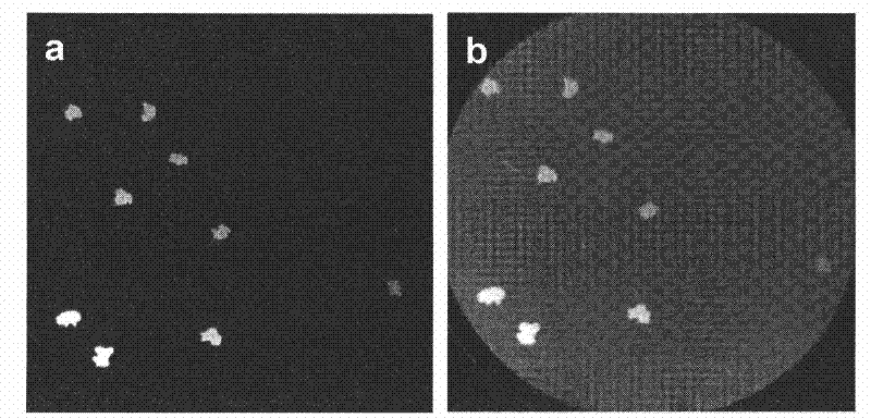
[0038] A monolayer graphene structure is grown on the Ru(0001) single crystal surface. The graphene / Ru(0001) surface was studied by PEEM imaging using Hg lamp light source and deep ultraviolet laser (177nm) as excitation light source respectively. image 3 (a) and (b) are PEEM images recorded with Hg lamp light source and deep ultraviolet laser (177nm) as excitation light source, respectively. Image size is 10 microns. Only the graphene structure exhibits a higher gray scale when excited by the Hg lamp, and the photoelectron signal on the surface of the Ru substrate is weaker, appearing as a dark area, and its surface structure cannot be distinguished. A deep ultraviolet laser was used to excite the surface because its higher energy can simultaneously excite photoelectron emission from the graphene and Ru surface regions. Laser PEEM realizes the ability to distinguish the surface structure of the two structures at the same time. This implementation case shows that the deep ...

Embodiment 2

[0040] A monolayer graphene structure is grown on the Ru(0001) single crystal surface. The PEEM imaging study of graphene / Ru(0001) surface was carried out with deep ultraviolet laser (177nm) as excitation light source. Figure 4 PEEM images excited by deep-UV laser without energy resolution (a) and with energy resolution (b). Image size is 10 microns. Using an energy analyzer can selectively pass photoelectrons with specific energies, which can further improve the contrast and resolution of PEEM images. This result shows that the energy-resolved PEEM image contrast is greatly improved (b), while the non-energy-resolved PEEM image has poor contrast in the graphene and Ru regions. This implementation example demonstrates that energy resolution can be achieved with an energy analyzer, further improving the quality of PEEM imaging.

Embodiment 3

[0042] The Si(001) with surface reconstruction is used as the sample, and the low-energy electron beam is used as the excitation source to form a LEEM image. Figure 5 Low-energy electron microscopy (LEEM) images excited by a low-energy electron beam with aberration correction (a) and without aberration correction (b). Image size is 0.6 microns. This result shows that the spatial resolution of LEEM with aberration correction function reaches 2.08nm, and the resolution without aberration correction function is 7.6nm. The reduction in spatial resolution caused by spherical and chromatic aberrations is reduced after the introduction of the aberration corrector. This implementation case illustrates the important role of the aberration corrector in improving the imaging quality, especially the spatial resolution, in the PEEM technique.


PUM


Abstract

The invention relates to a high-spatial-resolution photoemission electron microscope (PEEM) with an ultraviolet or deep ultraviolet laser light source, comprising an ultraviolet or deep ultraviolet laser and a PEEM, wherein an optical path of laser emitted by the ultraviolet or deep ultraviolet laser is vertically incident to a sample stage of the PEEM. (Deep) ultraviolet laser with fixed wavelength or continuous wavelength and energy higher than 5eV is applied to the PEEM; the laser arouses photoelectrons on the surface of a solid in a unique way of being vertically incident to the surface of a sample through a laser and PEEM connecting system; surface photoemission electrons are imaged by using an electron optical system so that surface image information is obtained; and dynamic processes including surface chemical reaction and a surface growth process on the surface of the solid are researched by applying the deep ultraviolet laser, so that high-spatial-resolution, in-situ and real-time research and observation of the dynamic processes of the surface are realized.

Description

technical field [0001] The present invention relates to new technologies and new methods of surface science research, specifically adopts ultraviolet and deep ultraviolet lasers as excitation light sources, utilizes the characteristics of high energy and high intensity of ultraviolet lasers to develop high spatial resolution photoemission electron microscopy (PEEM) ), used in surface science research and application fields such as surface chemistry, surface physics, thin film growth, and integrated circuits. Background technique [0002] Photoemission Electron Microscopy (PEEM) is a new surface analysis technique developed around the 1990s. It uses ultraviolet light or X-ray light to excite electrons in atoms on the surface of a solid, and uses an electron optical lens system to record photoelectron emission and image it. Compared with the main surface imaging techniques such as scanning electron microscope (SEM), scanning tunneling microscope (STM) and scanning Auger micro...

Claims


Application Information

Patent Timeline
Patent Type & Authority Applications(China)
IPC IPC(8): H01J37/26H01J37/02
Inventor 傅强金立谭大力慕仁涛包信和
Owner DALIAN INST OF CHEM PHYSICS CHINESE ACAD OF SCI
Why Eureka
Try Eureka