
Protector chip of light emitting diode and production technology thereof

A technology of light-emitting diodes and protection devices, which is applied in the field of protection device chips and production processes of light-emitting diodes, can solve problems such as inability to use light-emitting diodes to protect devices, low working voltage of light-emitting diodes, and inability to illuminate circuits, so as to improve reliability and anti-corrosion Surge capability, strong automatic recovery ability after circuit power failure, and fast switching speed

Active Publication Date: 2012-06-13
TIANJIN ZHONGHUAN SEMICON CO LTD
View PDF1 Cites 8 Cited by
  • Summary
  • Abstract
  • Description
  • Claims
  • Application Information

AI Technical Summary

Problems solved by technology

[0002] Because light-emitting diodes (LEDs) have the characteristics of low operating voltage, small operating current, uniform and stable light emission, and environmental protection, they are currently widely used in automotive headlights, equipment indicator lights, and various lighting circuits. Multiple light-emitting diodes are connected in series, and one damage will affect the entire circuit and cannot be illuminated.
There is no low-voltage, fast-triggering thyristor bidirectional overvoltage protection device specially designed for light-emitting diodes in the semiconductor industry. Most of the existing thyristor devices on the market are high-power, high-voltage rectifying devices, which cannot Protection devices for light-emitting diodes

Method used


Image

  • Protector chip of light emitting diode and production technology thereof
  • Protector chip of light emitting diode and production technology thereof
  • Protector chip of light emitting diode and production technology thereof

Examples


Embodiment Construction

[0027] In order to understand the present invention more clearly, describe the present invention in detail in conjunction with accompanying drawing:

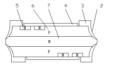
[0028] The protection device chip structure of the light emitting diode is N-P-N-P-N type.

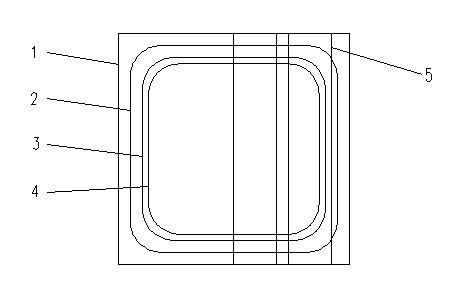
[0029] Such as figure 1 The planar structure of the chip of the protection device of the light-emitting diode is as follows: chip 1, corrosion groove 2, passivation glass 3, metal layer 4, high-concentration N region 5;

[0030] Such as figure 2 The chip sectional structure of the protection device of the light emitting diode shown is as follows: corrosion trench 2, passivation glass 3, metal layer 4, high-concentration N region 5, P region 6, and base region N7.

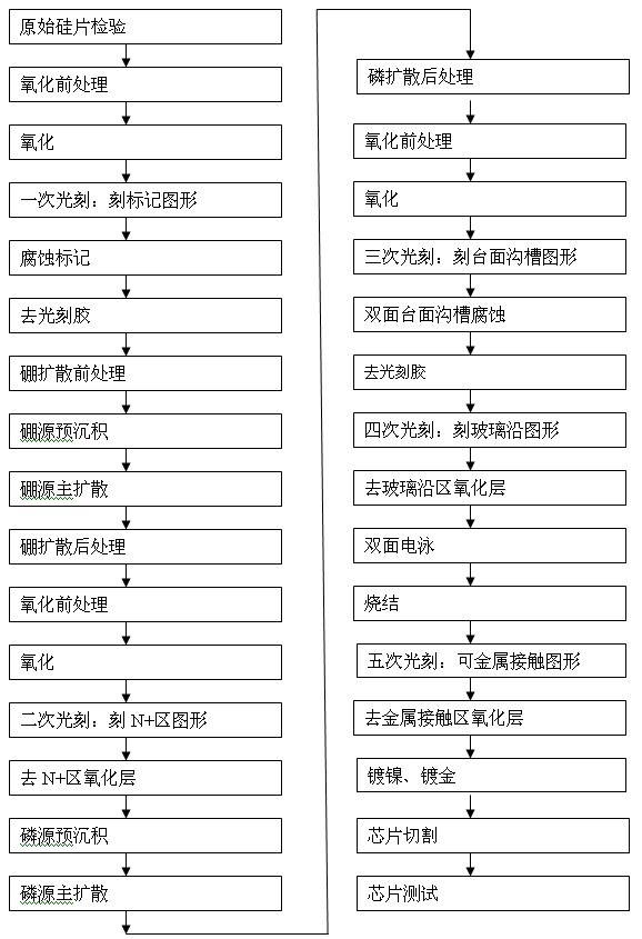
[0031] Such as image 3 The chip process flow of the protective device for the light emitting diode shown is as follows:

[0032] 1) Pre-oxidation treatment: chemically treat the surface of silicon wafers through acid, alkali, deionized water and other processes;

[...


PUM


Abstract

The invention relates to a protector chip of a light emitting diode and production technology thereof. Through employing a narrow substrate base region width structure, bulk voltage drop is decreased, switching speed is raised, and switching loss is reduced; a diffusion method that gas carries a shallow N+ junction of liquid phosphor source is employed, depth and concentration gradient of a diffused junction are controlled well, stability of breakdown voltage is increased with good elasticity, a device is conducted rapidly, and a role of protecting the light emitting diode is played; evenness and homogeneity of the diffused junction are increased, and reliability and antisurge capability of a protection tube are raised; electrophoretic glass passivation technology is employed, stability of trigger voltage and breakdown voltage of the protection tube is raised, the protection tube of the light emitting diode has the characteristics of fast switching speed, strong automatic recovery capability of circuit power failure and low loss, when a light emitting diode is in a open circuit state, conduction can be carried out rapidly, which does not cause collapse of a whole light emitting diode matrix, a circuit can continue to work, and a reliable illumination function is provided for a high frequency highlight brightness circuit.

Description

technical field [0001] The invention relates to the technical field of chip production of low-voltage trigger protection devices, in particular to a chip and a production process of a bidirectional protection device specially protecting light-emitting diodes. Background technique [0002] Because light-emitting diodes (LEDs) have the characteristics of low working voltage, small working current, uniform and stable light emission, and environmental protection, they are currently widely used in automobile headlights, equipment indicator lights and various lighting circuits, but their disadvantages are that in the circuit Multiple light-emitting diodes are connected in series, and if one is damaged, the entire circuit cannot be illuminated. There is no low-voltage, fast-triggering thyristor bidirectional overvoltage protection device specially designed for light-emitting diodes in the semiconductor industry. Most of the existing thyristor devices on the market are high-power, h...

Claims


Application Information

Patent Timeline
IPC IPC(8): H01L27/02H01L21/822
Inventor 刘长蔚王军明初亚东王智伟白树军杨玉聪刘玉涛闫禹
Owner TIANJIN ZHONGHUAN SEMICON CO LTD
Learn More