Preparation device for preparing functional micro-nano materials on silicon surfaces based on femtosecond laser and method

A femtosecond laser and preparation device technology, which is applied in the manufacture of microstructure devices, processes for producing decorative surface effects, microstructure devices, etc., can solve problems such as the limitation of the bandgap width of the absorption rate of silicon materials, and reduce heat dissipation. Damage, speed-up effects

Inactive Publication Date: 2012-06-20
CHANGCHUN UNIV OF SCI & TECH
View PDF5 Cites 36 Cited by
  • Summary
  • Abstract
  • Description
  • Claims
  • Application Information

AI Technical Summary

Problems solved by technology

[0004] In order to solve the problem that the absorption rate of existing silicon materials is limited by the forbidden band width, the present invention provides a device and method for preparing silicon surface functional micro-nano materials based on femtosecond laser, which can process the surface of ordinary silicon materials with high efficiency , and then obtain a new type of silicon material with micro-nano structure and high absorption rate on the surface

Method used


Image

  • Preparation device for preparing functional micro-nano materials on silicon surfaces based on femtosecond laser and method
  • Preparation device for preparing functional micro-nano materials on silicon surfaces based on femtosecond laser and method
  • Preparation device for preparing functional micro-nano materials on silicon surfaces based on femtosecond laser and method

Examples


Embodiment 1

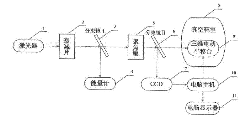
[0037] The preparation device and method of femtosecond laser-based silicon surface functional micro-nano materials of the present invention include: a laser 1, an attenuation plate 2, a first beam splitter 3, an energy meter 4, a focusing mirror 5, a second beam splitter 6, CCD7, vacuum target chamber 8, three-dimensional electric translation stage 9, computer mainframe 10 and display 11; wherein laser 1 is connected with attenuation sheet 2, first beam splitter mirror 3, focusing mirror 5, the first on the optical axis of its output beam in sequence Two beam splitters 6, a vacuum target chamber 8, and a three-dimensional electric translation platform 9.

[0038] The second beam splitting mirror 6 is connected with the energy meter 4; the focusing mirror 5 is connected with the CCD7; the CCD7 is connected with the computer host 10; the three-dimensional electric translation platform 9 is connected with the computer host 10;

[0039] Laser 1 is a femtosecond laser with a pulse...

Embodiment 2

[0055] Charge SF in step 2 6 The etching gas pressure is 10kPa; the rest are the same as in Embodiment 1.

Embodiment 3

[0057] Charge SF in step 2 6 The etching gas pressure is 20kPa; the rest are the same as in Embodiment 1.


PUM

PropertyMeasurementUnit
wavelengthaaaaaaaaaa
thicknessaaaaaaaaaa
electrical resistivityaaaaaaaaaa

Abstract

The invention provides a preparation device for preparing functional micro-nano materials on silicon surfaces based on femtosecond laser and a method. When the device is used for preparation, scanning speed reaches 4mm/s, and is increased by 20 times as compared with scanning speed when micro-nano materials are prepared in a traditional method. Simultaneously, supersaturation doping of the silicon material surface and preparation of micro-nano structures of the surfaces are realized during preparation, prepared micro-nano materials can absorb 90% of light with wavelength ranging from 200nm to 2500nm, and silicon materials without scanning traces on surfaces can be obtained. The preparation device and the method are exquisite in design and easy to control, and the prepared materials can be applied to solar cells, detectors, field emission devices and the like in the photoelectric industry.

Description

technical field [0001] The invention relates to a femtosecond laser-based silicon surface functional micro-nano material preparation device and method, which belongs to the technical field of silicon-based semiconductor photoelectric materials, and the application field includes optoelectronic industries such as solar cells, detectors, and field emitters. Background technique [0002] Inexpensive silicon is now widely used as a substrate for semiconductor microelectronics. From computer chips to light detectors, silicon has opened up many commercial applications. However, due to the limitation of the band gap (1.07eV) of the silicon material itself, its ability to absorb and photoelectrically convert infrared (>1.1 μm) is fundamentally limited. In 1997, the research group of Professor Mazur of Harvard University found that the use of femtosecond laser (100fs) to irradiate silicon wafers in a certain gas environment can produce micron-scale peak structure. [Appl. Phys. L...

Claims


Application Information

Patent Timeline
Patent Type & Authority Applications(China)
IPC IPC(8): B23K26/12B23K26/08B23K26/02B81C1/00B23K26/064B23K26/082
Inventor 林景全谭欣陶海岩
Owner CHANGCHUN UNIV OF SCI & TECH
Why Eureka
Try Eureka