High-speed terahertz modulator and production method thereof

A production method and terahertz technology, applied in the field of terahertz wave communication, can solve problems such as short life and limitations, and achieve the effect of reducing requirements and facilitating modulation rate

Inactive Publication Date: 2012-06-27
SOUTHEAST UNIV
View PDF4 Cites 24 Cited by
  • Summary
  • Abstract
  • Description
  • Claims
  • Application Information

AI Technical Summary

Problems solved by technology

However, due to the short lifetime of carriers in GaAs, the response time can reach the order of 130 ps, ​​so although the modulation rate of the THz wave can reach the order of GHz in theory, in order to obtain a higher concentration of photogenerated carriers and a higher Large modulation depth, the luminous flux of the 810 nm modulated laser needs to reach an extremely high level of 0.8 μJ / cm2, and the corresponding continuous wave output laser power needs to reach 105 W above, which makes it extremely limited in practical applications

Method used


Image

  • High-speed terahertz modulator and production method thereof
  • High-speed terahertz modulator and production method thereof
  • High-speed terahertz modulator and production method thereof

Examples


Embodiment Construction

[0023] The present invention will be further explained below in conjunction with the accompanying drawings and specific embodiments. It should be understood that these embodiments are only used to illustrate the present invention and are not intended to limit the scope of the present invention. After reading the present invention, those skilled in the art all fall into the appended claims of the present application to the amendments of various equivalent forms of the present invention limited range.

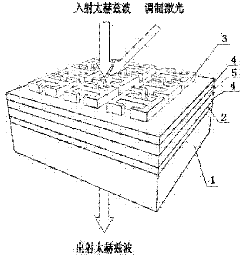
[0024] Such as figure 1 As shown, a terahertz wave high-speed modulator includes a -oriented semi-insulating gallium arsenide (GaAs) substrate layer 1. First, a GaAs buffer layer 2 is grown on the substrate by MOCVD metal organic chemical vapor phase epitaxy technology. The thickness of the gallium arsenide buffer layer 2 is controlled at 20 to 300 nanometers, so that the large difference in lattice constant between the indium gallium arsenide potential well layer 5 and the gall...


PUM

PropertyMeasurementUnit
thicknessaaaaaaaaaa
thicknessaaaaaaaaaa
thicknessaaaaaaaaaa

Abstract

The invention discloses a high-speed terahertz modulator and a production method thereof. The terahertz high-speed modulator comprises a substrate layer, a buffer layer growing on the substrate layer, a strained quantum well structure growing on the buffer layer and a metal meta-material structure, wherein the metal meta-material structure is prepared on the upper surface of the strained quantum well structure and consists of a periodical array of metal resonant units. Besides, the buffer layer and the substrate layer are made of the same materials, the band gap of a potential well layer is smaller than that of a potential barrier layer, and the difference between the lattice constants of the potential barrier layer and the substrate layer is controlled within 0.5%. A strong piezoelectric field generated from strain is formed in strained quantum well structure, and accordingly recombination lifetime of photon-generated carriers is prolonged and concentration thereof is increased evidently, and requirements for power of a modulated laser are lowered greatly. By changing the In component and quantum well width in the InGaAs/GaAs strained quantum well structure, the strength of the piezoelectric field inside and charge spatial isolation degree can be regulated flexibly, and accordingly the modulation rate of the high-speed terahertz modulator can be regulated conveniently.

Description

[0001] technical field [0002] The invention belongs to the field of terahertz wave communication, and in particular relates to a terahertz wave modulator and a manufacturing method thereof. Background technique [0003] The contradiction between the limited spectrum resources of wireless communication and the rapidly growing high-speed business demands forces people to develop new spectrum bands. Terahertz waves refer to electromagnetic waves with frequencies ranging from 0.1 THz to 10 THz (1 THz = 10 12 Hz), the wavelength is 0.03 mm to 3 mm, and has a large bandwidth, so the development of THz wireless communication technology has important practical application value. Among them, the terahertz wave modulator is one of the essential devices in the terahertz communication system, but the performance of the terahertz modulator is mainly limited by the selection and preparation of materials. The organic combination of new semiconductor substrate materials and electromagn...

Claims


Application Information

Patent Timeline
Patent Type & Authority Applications(China)
IPC IPC(8): G02F1/017H01S5/343
Inventor 张雄丛嘉伟郭浩崔一平
Owner SOUTHEAST UNIV
Why Eureka
Try Eureka