Machining method of semiconductor chip

A processing method and semiconductor technology, applied in the direction of semiconductor devices, etc., can solve problems such as no reports on chips, and achieve the effects of short pickling time, small corrosion amount, and easy implementation.

Active Publication Date: 2014-03-12
合肥协鑫集成光电科技有限公司
View PDF4 Cites 0 Cited by
  • Summary
  • Abstract
  • Description
  • Claims
  • Application Information

AI Technical Summary

Problems solved by technology

However, the technical means of making chips by cracking wafers into regular hexagons has never been reported in the prior art.

Method used


Image

  • Machining method of semiconductor chip
  • Machining method of semiconductor chip
  • Machining method of semiconductor chip

Examples


Embodiment Construction

[0040] The processing method of the present invention is as Figure 1-5 shown, including the following steps:

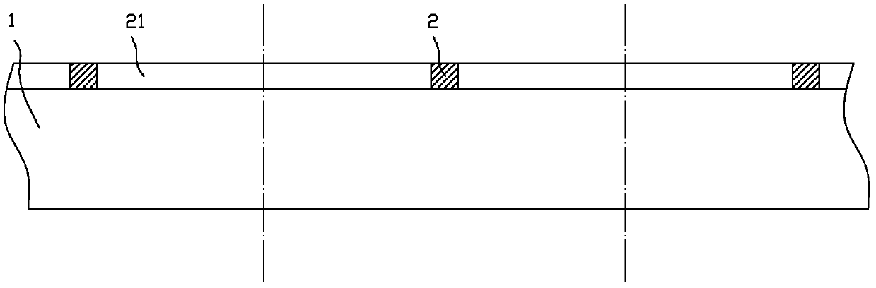
[0041] Diffusion is performed on wafer 1;

[0042] The process of setting the oxide layer 2 and photoetching the window 21 on the oxide layer 2; figure 1 ;

[0043] After the photoetching window 21, the oxide layer 2 is grid-like on the wafer surface; the internal shape of the grid is as follows: Figure 17-20 , can be a circle, a square with rounded corners, a regular hexagon or a regular octagon, and the above-mentioned planar shape can be formed during the production of the masking film according to the needs of the specific application environment.

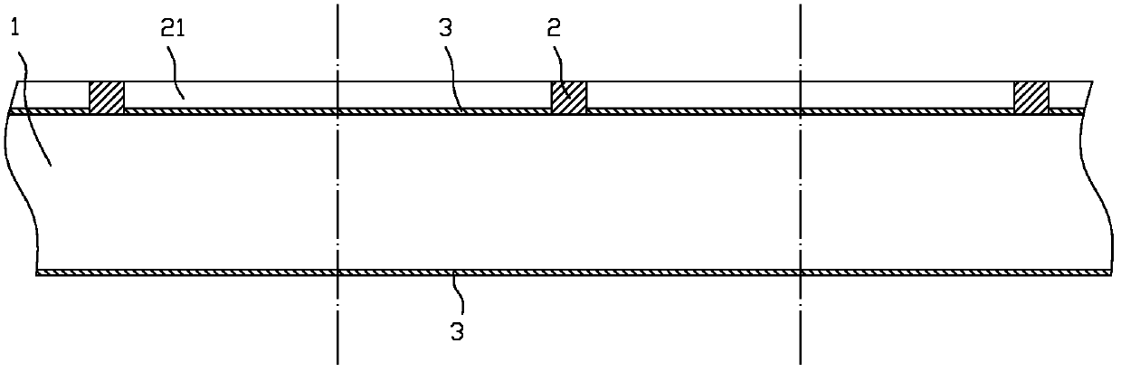
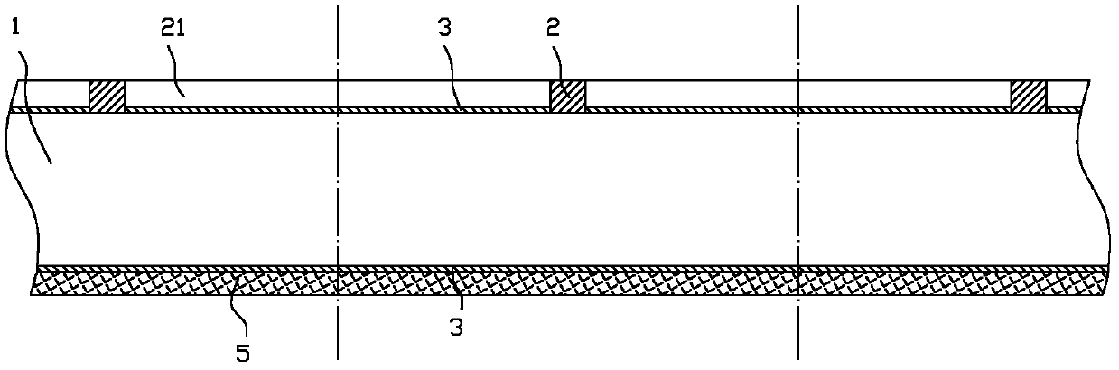
[0044] Then process as follows:

[0045] 1), set the electrode layer; such as figure 2 , coating the metal electrode layer 3 on the wafer surface in the window 21; as an electrode;

[0046] 2) One-time acid etching: using hydrofluoric acid to remove the grid-like oxide layer 2 grid on the surface of the wafer ...


PUM


Abstract

The invention discloses a machining method of a semiconductor chip, relating to a splitting process without mechanical damage, and provides a machining method of the semiconductor chip, which has the advantages of high efficiency and no mechanical damage and provides a friendly linkage measure. The machining method comprises the following steps of: 1, setting an electrode layer; 2, once acid-etching; and 3, secondarily acid-etching. According to the machining method, an electrode window is firstly formed, and then a metal electrode layer is coated and planted on the electrode window on the surface of a wafer. The metal electrode does not basically react with acid in processes of two times of acid etching. A strong chemical reaction exists between strong acid and a wafer body made of silicon, the wafer body can be rapidly etched, and further the wafer is split according to a designed shape, and finally, hexagonal, circular and other-shaped chips which are difficult to obtain by adopting common means are finally machined.

Description

technical field [0001] The invention relates to a semiconductor chip manufacturing method, in particular to a cracking process without mechanical damage. Background technique [0002] The existing OJ (Open Juction) type diode manufacturing method mainly includes the following steps: Diffusion to form a semiconductor wafer with the required vertical structure; Nickel plating; Cutting into square or regular hexagonal single chips; The wire and the metal electrode layer of the chip are welded and assembled together; pickled with mixed acid; glued and cured to form a passivation protective layer; epoxy molded and cured; pins are tinned; test package. The chips used in this method are generally square after cutting, and the corners are 90°. The electric field strength is stronger at the sharp corners, and it is easy to break down and fail. If it is cut into a regular hexagon, there will be a certain area waste, especially for large This contradiction is particularly prominent fo...

Claims


Application Information

Patent Timeline
Patent Type & Authority Patents(China)
IPC IPC(8): H01L21/28
Inventor 薛列龙
Owner 合肥协鑫集成光电科技有限公司
Why Eureka
Try Eureka