Multiple epitaxial growth method for realizing big length-to-diameter ratio ZnO nanowire array film based on low-temperature hydrothermal method

A nanowire array, large aspect ratio technology, applied in liquid phase epitaxy layer growth, polycrystalline material growth, single crystal growth and other directions, can solve the problem of high growth temperature

Inactive Publication Date: 2012-07-04
XI AN JIAOTONG UNIV
View PDF1 Cites 7 Cited by
  • Summary
  • Abstract
  • Description
  • Claims
  • Application Information

AI Technical Summary

Problems solved by technology

There are also reports that the length of nanowires increases approximately linearly with growth time at temperatures higher than 80°C. However, due to the high growth temperature, the outer diameter of nanowires also increases linearly at the same time, which cannot achieve the desired results in device application research as the growth time increases. Large aspect ratio nanowire array requirements

Method used


Image

  • Multiple epitaxial growth method for realizing big length-to-diameter ratio ZnO nanowire array film based on low-temperature hydrothermal method
  • Multiple epitaxial growth method for realizing big length-to-diameter ratio ZnO nanowire array film based on low-temperature hydrothermal method
  • Multiple epitaxial growth method for realizing big length-to-diameter ratio ZnO nanowire array film based on low-temperature hydrothermal method

Examples


Embodiment Construction

[0024] Concrete implementation steps of the present invention are as follows:

[0025] 1. Silicon substrate cleaning. The cleaning of the silicon substrate follows the principle of cleaning the organic matter first, and then cleaning the inorganic matter, and proceeds according to the process of supersonication (ultrasonic), boiling (acid boiling), and rinsing (rinsing).

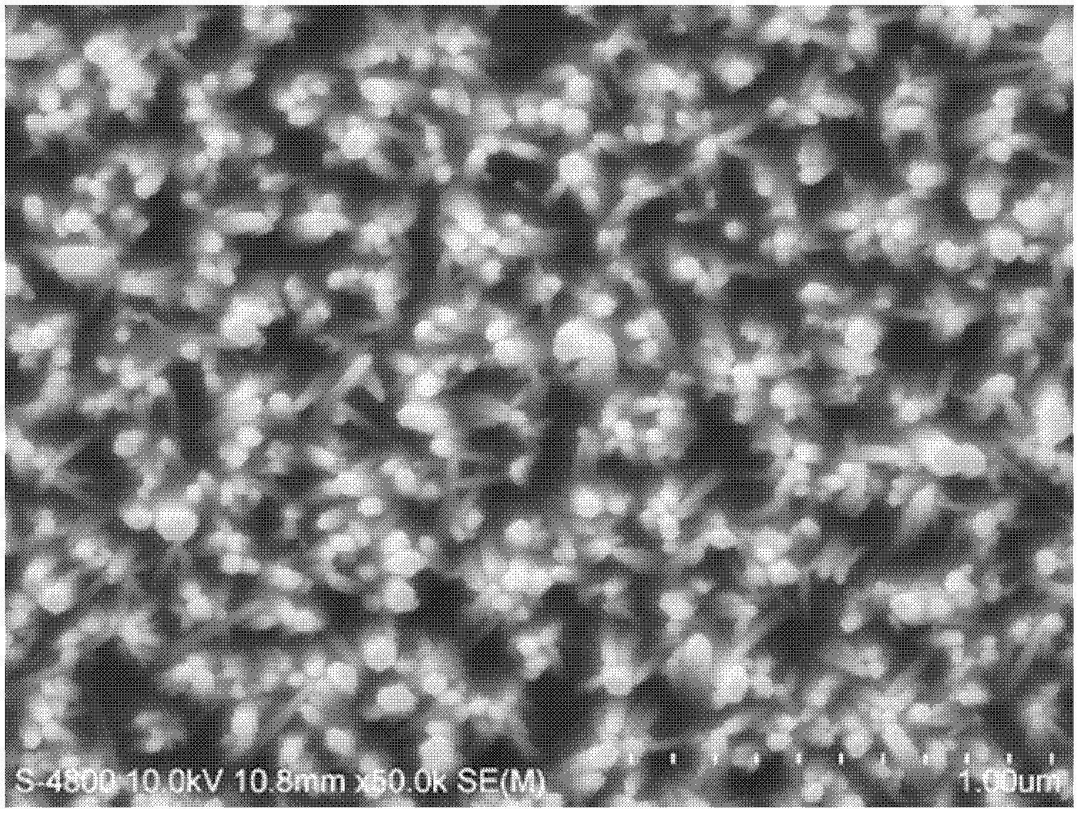
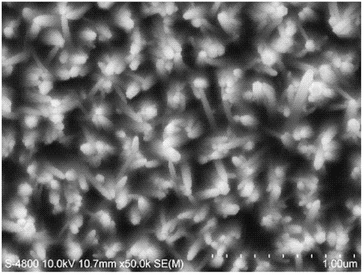
[0026] 2. Sputtering deposition of ZnO nano-seed layer. ZnO nano-seed layer was deposited by radio frequency magnetron sputtering process of ZnO ceramic target. The main process parameters are: vacuum degree 6E -4 Pa, oxygen flow: 5sccm, argon flow: 10sccm, radio frequency power: 120W, sputtering pressure: 1.0Pa, substrate heating temperature: 25080°C, sputtering time: 30min.

[0027] 3. Single self-assembly growth of ZnO nanowires. Form a mixed solution of 0.025mol / L zinc acetate dihydrate solution and hexamethylenetetraammonium solution at a volume ratio of 1:1, suspend the seed crystal film obtained i...


PUM


Abstract

The invention relates to a multiple epitaxial growth method for realizing a big length-to-diameter ratio ZnO nanowire array film based on a low-temperature hydrothermal method, which comprises the following steps: carrying out sputtering deposition on a ZnO nano seed crystal layer on a silicon substrate; taking the ZnO nano seed crystal layer as a guiding layer, realizing the growth of a ZnO nanowire vertical orientation array by utilizing the hydrothermal method and controlling the growth time within 3 hours; and cleaning the sample, carrying out secondary epitaxial growth on the ZnO nanowire array single growth sample by applying again the hydrothermal method and controlling the growth time within 3 hours. According to the invention, the wet epitaxial growth of the top end of a single ZnO nanowire along the (0001) direction is realized, the length-to-diameter ratio of the nanowire is greatly increased, and the appearance of the growth saturation phenomenon as the increase of growth time under the single growth condition of the ZnO nanowire is overcome.

Description

Technical field: [0001] The invention patent relates to the field of controllable preparation of ZnO semiconductor nanostructures, and the controllable preparation of ZnO semiconductor nanostructures is the experimental basis for its application research. It specifically involves the use of secondary epitaxial growth of ZnO nanowires to realize the low-temperature hydrothermal growth method of ZnO nanowire array films with a large aspect ratio. The method has strong applicability and can be realized on various substrates such as single crystal silicon, quartz and glass. . Background technique: [0002] Since Peidong Yang, Department of Chemistry, University of California, Berkeley, reported the phenomenon of ZnO nanowire ultraviolet laser emission in Science in 2001, one-dimensional ZnO nanostructures have received extensive attention as one of the frontiers in the field of ZnO new wide bandgap semiconductors. , the controllable preparation method is not only the basis of Z...

Claims


Application Information

Patent Timeline
Patent Type & Authority Applications(China)
IPC IPC(8): C30B29/16C30B29/62C30B19/00
Inventor 贺永宁康雪张雯彭文博
Owner XI AN JIAOTONG UNIV
Why Eureka
Try Eureka