All-optical logic gate device based on nanowire waveguides of multislot silicon substrate

A nanowire, optical logic technology, applied in the field of integrated optics, can solve the problems of difficult to achieve ultra-high-speed all-optical logic operation, impractical design of all-optical logic gates, weak nonlinear effects of silicon-based materials, etc. Optical power requirements, the realization of optical signal processing, the effect of cheap structural materials

Inactive Publication Date: 2012-07-04
SOUTHEAST UNIV
3 Cites 6 Cited by

AI-Extracted Technical Summary

Problems solved by technology

The all-optical logic gate based on the SOI waveguide structure mainly uses the nonlinear optical effect of the silicon-based material to change the effective refractive index of the waveguide material to control the transmitted signal light, thereby realizing various logic operations. However, the operating speed of the logic gate will be limited by the current carrying capacity. Due to the l...

Method used

The three-groove vertical silicon-based nanowire waveguide is composed of four close silicon-based nanowires (i.e. buried rectangular waveguides) with high refractive index distribution difference, and three grooves (i.e. nanoscale low refractive index distribution area) are formed in the middle, According to the boundary value relationship of the electromagnetic field, the electric field component perpendicular to the interface of the material with high refractive index difference distribution will appear discontinuous, because the width of the groove (on the order of nanometers) is much smaller than the characteristic attenuation length of the rectangular waveguide, making the low refractive index The electric field in the slot is greatly enhanced. Compared with the single-slot waveguide structure, the three-slot vertical silicon-based nanowire waveguide structure has a stronger light field confinement ability, but the number of grooves is larger, and the light field confinement ability is not significantly improved. The realization feature of the all-optical logic gate is that due to the strong polarization dependence of the slot waveguide structure, the quasi-transverse electric mode is strictly confined in the nonlinear slot, while ...

Abstract

The invention discloses an all-optical logic gate device based on nanowire waveguides of a multislot silicon substrate, which is characterized by comprising two input waveguides, two output waveguides, first mode converters (51), a nonlinear directional coupler (6) and second mode converters (52). The input waveguides include a first input waveguide (1) and a second input waveguide (2) and are used for inputting signal optical pulses and controlling the optical pulses, the output waveguides include a first output waveguide (3) and a second output waveguide (4), the first input waveguide (1) and the second input waveguide (2) are respectively connected with the nonlinear directional coupler (6) by the first mode converters (51), and the nonlinear directional coupler (6) is respectively connected with the first output waveguide (3) and the second output waveguide (4) by the second mode converters (52). The all-optical logic gate device has the advantages of easiness in implementation, fast working speed, low power consumption, compact structure, cheap price and the like.

Application Domain

Logic circuits using opto-electronic devicesOptical light guides +1

Technology Topic

Optical logic gatesConverters +5

Image

  • All-optical logic gate device based on nanowire waveguides of multislot silicon substrate
  • All-optical logic gate device based on nanowire waveguides of multislot silicon substrate
  • All-optical logic gate device based on nanowire waveguides of multislot silicon substrate

Examples

  • Experimental program(1)

Example Embodiment

[0026] The principles and features of the present invention will be described below with reference to the accompanying drawings. The examples are only used to explain the present invention, but not to limit the scope of the present invention.
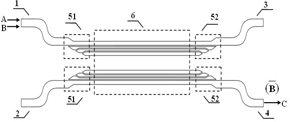
[0027] The present invention adopts the following technical solutions. An all-optical logic gate device based on a multi-slot silicon-based nanowire waveguide includes: two input waveguides 1 and 2 capable of inputting signal optical pulses and control optical pulses, and two output waveguides 3 , 4, mode converters 51, 52, nonlinear directional coupler 6, wherein the connection parts between the input waveguides 1, 2 and output waveguides 3, 4 and the nonlinear directional coupler 6 are the first mode converter 51 and the second The mode converter 52 realizes the mode conversion between the input waveguides 1, 2 and the output waveguides 3, 4 and the three-slot vertical silicon-based nanowire waveguide. The nonlinear directional coupler 6 is composed of the three-slot vertical silicon-based nanowire waveguide in the slot. filled with non-linear materials.
[0028] The three-slot vertical silicon-based nanowire waveguide is composed of four close silicon-based nanowires with high refractive index distribution difference (ie, buried rectangular waveguides), and three grooves (ie, nano-scale low-refractive index distribution regions) are formed in the middle. According to the electromagnetic field The boundary value relationship, the electric field component perpendicular to the material interface with high refractive index difference distribution will appear discontinuous, because the width of the groove (in the order of nanometers) is much smaller than the characteristic attenuation length of the rectangular waveguide, so that the low refractive index in the groove The electric field is greatly enhanced. Compared with the single-slot waveguide structure, the three-slot vertical silicon-based nanowire waveguide structure has stronger optical field confinement ability, but the number of grooves is more, and the optical field confinement ability is not improved significantly. The realization feature of the all-optical logic gate is: due to the strong polarization dependence of the slot waveguide structure, the quasi-transverse electrical mode is strictly confined in the nonlinear slot, while the quasi-transverse magnetic mode diffuses into the silicon nanowire cladding Therefore, the propagation characteristics of the quasi-transverse electric mode and the quasi-transverse magnetic mode in the nonlinear slot waveguide are quite different. When only the quasi-transverse magnetic mode is incident into the nonlinear directional coupler, its propagation is the same as the linear case. When When the quasi-transverse electric mode and the quasi-transverse magnetic mode are incident at the same time, because the quasi-transverse electric mode is well confined in the nonlinear groove of low refractive index, it is affected by the nonlinear effect, and the propagation characteristics of the quasi-transverse electric mode are different from the linearity. Under different conditions, it will cause the phase change of the quasi-transverse magnetic mode signal input at the same time, resulting in phase mismatch, changing the coupling state, and thus controlling the output optical field to switch between the two output ports of the directional coupler. By changing the optical polarization mode of the input signal and the combined state of the corresponding input port, the output waveguide can output different logic effects correspondingly and realize different logic functions.
[0029] The invention discloses an all-optical logic gate device based on a multi-slot silicon-based nanowire waveguide, and aims to provide an all-optical logic gate design with simple processing technology, compact structure, excellent performance and easy integration, which can be used for optical information processing. , optical communications and integrated optics. The device includes two input waveguides for inputting signal optical pulses and control optical pulses, namely the first input waveguide 1 and the second input waveguide 2, and two output waveguides, namely the first output waveguide 3 and the second output waveguide 4 , the first mode converter 51, the nonlinear directional coupler 6, the second mode converter 52, where
[0030] The first input waveguide 1 and the second input waveguide 2 are respectively connected to the nonlinear directional coupler 6 through the first mode converter 51 , and the nonlinear directional coupler 6 is respectively connected to the first output waveguide 3 and the first output waveguide 3 through the second mode converter 52 . Two output waveguides 4 are connected.
[0031] The input states of the input waveguide and the polarization modes of the input optical field determine various logical functions such as "NO", "AND" and "OR" corresponding to the output of the output waveguide.
[0032] refer to figure 1 , which shows the configuration of the "NO" logic gate of the present invention, and its working principle is as follows: the signal A and the signal B with the optical power P are simultaneously incident on the first input waveguide 1, and the signal enters the first input waveguide 1 through the first mode converter 51. The nonlinear directional coupler 6 finally outputs the signal to the second output waveguide 4 through the second mode converter 52 . In the design, the signal A is a quasi-transverse magnetic mode, the signal B is a quasi-transverse electric mode, and the signal power P is greater than the threshold power that can cause nonlinear phase mismatch. When the pulse of the signal A is "1" and the pulse of the signal B is "0", the signal A is output from the second output waveguide 4 through the nonlinear directional coupler 6, that is, the signal C is "1"; when the signal A and the signal When the pulses of B are all "1", since the quasi-transverse electrical mode is well confined in the slot of the three-slot vertical silicon-based nanowire waveguide, it is in full contact with the nonlinear material in the slot. Linear effect, resulting in nonlinear phase shift of the light field propagating in the three-slot vertical silicon-based nanowire waveguide, therefore, the quasi-transverse electrical mode, that is, the signal B, will not be output from the second output waveguide 4, and at the same time, the signal B is in the The nonlinear perturbation is superimposed on the signal A, which causes the phase mismatch of the signal A, so that the signal A will not be coupled into the second output waveguide 4, that is, the signal C is "0". So in this case, , that is, the “NO” NOT logic function is realized, and its logic value is output from the second output waveguide 4 . Table 1 shows its truth table. figure 2 It is a cross-sectional view of the nonlinear directional coupler 6. The nonlinear directional coupler 6 is composed of three-slot vertical silicon-based nanowire waveguides. The selection of the structural parameters of the line waveguide can ensure that the directional coupler formed by the directional coupler has the same coupling length for the quasi-transverse electric mode and the quasi-transverse magnetic mode under linear conditions, and the length of the nonlinear directional coupler 6 is selected to be an integer multiple of the coupling length. . Figure 3a and Figure 3b The mode field distribution diagrams of the electric field principal components of the quasi-transverse electric mode and the quasi-transverse magnetic mode carried by the three-slot vertical silicon-based nanowire waveguide structure, and the electric field principal component of the quasi-transverse electric mode E x well confined in the three low-refractive-index grooves, while the electric field principal component of the quasi-transverse magnetic mode E y Then it diffuses into the cladding of the slot waveguide structure. It can be seen that the structure has a strong optical field confinement ability for the quasi-transverse electric mode, while the optical field confinement ability for the quasi-transverse magnetic mode is weak, so it has a strong polarization. Correlation.
[0033] refer to Figure 4 , which shows the configuration of the "AND" and "OR" logic gates of the present invention, and its working principle is as follows: Signal A and signal B with optical power P are respectively incident on the first input waveguide 1 and the second input waveguide 2 , the two signals respectively enter the two incident ends of the nonlinear directional coupler 6 through the first mode converter 51 , and finally output the signals to the first output waveguide 3 and the second output waveguide 4 through the second mode converter 52 . In the design, the signal A is a quasi-transverse magnetic mode, the signal B is a quasi-transverse electric mode, and the signal power P is greater than the threshold power that can cause nonlinear phase mismatch. When the pulse of the signal A is "1" and the pulse of the signal B is "0", the situation is the same as the linear case, the signal A is output from the second output waveguide 4 through the nonlinear directional coupler 6, that is, the signal C is " 0", signal D is "1"; when the pulse of signal A is "0" and the pulse of signal B is "1", due to phase mismatch, signal B will not be coupled to the first after passing through the nonlinear directional coupler 6. In the first output waveguide 3, it is output from the second output waveguide 4, that is, the signal C is "0" and the signal D is "1"; when the pulses of the signal A and the signal B are both "1", due to the signal B The superimposed nonlinear perturbation, when the signal A propagates in the nonlinear directional coupler 6, is also not coupled into the second output waveguide 4 due to the phase mismatch, but is output from the first output waveguide 3, while the signal B Still output from the second output waveguide 4, that is, the signal C is "1" and the signal D is "1". Therefore, in this case, C=A·B, D=A+B, that is, the logical functions of "AND" AND "OR" OR are realized. The logical "AND" AND value is output from the first output waveguide 3, and the logical The OR value is output from the second output waveguide 4 . Table 2 shows its truth table.
[0034]
[0035] A B C 1 0 1 1 1 0
[0036] Table 1
[0037] A B C D 0 0 0 0 1 0 0 1 0 1 0 1 1 1 1 1
[0038] Table 2
[0039] The above are only preferred embodiments of the present invention and are not intended to limit the present invention. Any modification, equivalent replacement, improvement, etc. made within the spirit and principle of the present invention shall be included in the protection scope of the present invention. Inside.

PUM

no PUM

Description & Claims & Application Information

We can also present the details of the Description, Claims and Application information to help users get a comprehensive understanding of the technical details of the patent, such as background art, summary of invention, brief description of drawings, description of embodiments, and other original content. On the other hand, users can also determine the specific scope of protection of the technology through the list of claims; as well as understand the changes in the life cycle of the technology with the presentation of the patent timeline. Login to view more.

Similar technology patents

Anti-failure pneumatic window opener

ActiveCN109914958ASimple working principleThe structure is easy to disassemblePower-operated mechanismWing openersPistonAir spring
Owner:郑州洪华建筑科技有限公司

Classification and recommendation of technical efficacy words

  • Simple working principle
  • Easy to operate

Safety rod driving system of liquid heavy metal cooling reactor

Owner:HEFEI INSTITUTES OF PHYSICAL SCIENCE - CHINESE ACAD OF SCI
Why Eureka
Try Eureka